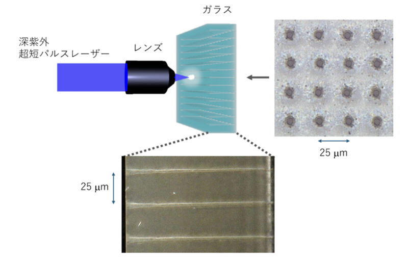
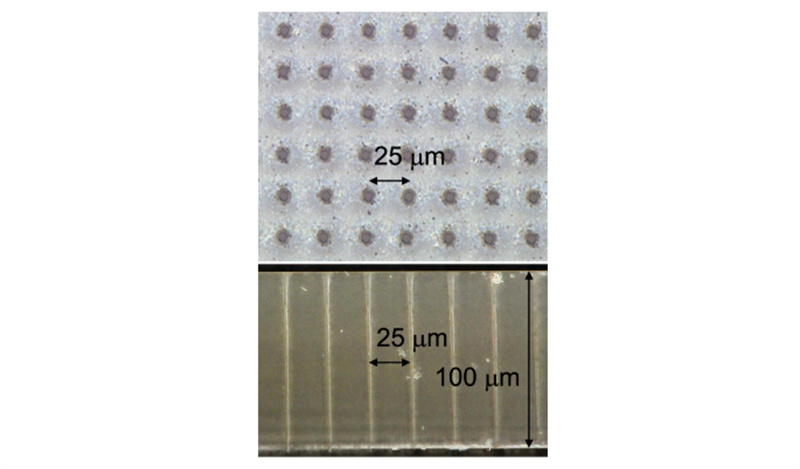
The University of Tokyo announced on May 31, 2025, that its research team has developed a high-precision laser drilling technique for glass substrates, enabling sub-10 μm via formation with aspect ratios up to 20—without cracks or chemical processing.
This breakthrough, presented at the 2025 IEEE 75th Electronic Components and Technology Conference (ECTC) held in Dallas from May 27, marks a significant step toward adopting glass as a next-generation material in semiconductor and PCB substrate applications. At the conference, the team presented their findings under the title: "High-aspect-ratio, 6-μm-diameter through-glass-via fabrication into 100-μm thick EN-A1 by dry laser micro-drilling process."

Glass substrates, such as AGC's EN-A1 used in the study, are emerging as promising candidates for high-density interposers and core substrates in advanced packaging due to their superior dielectric properties, thermal compatibility with silicon, and flatness over large areas. However, forming deep, narrow through-glass vias (TGVs) has long been a bottleneck due to glass's brittle nature.

By using a deep ultraviolet (DUV) ultrashort pulse laser, the University of Tokyo researchers achieved clean, high-aspect-ratio microvias directly through glass without cracks—surpassing the limitations of conventional acid-based etching methods. The laser-based method requires no chemical treatment, reducing environmental impact and simplifying manufacturing.

The demand for finer interconnects and larger-area substrates is rapidly growing as the semiconductor industry moves toward beyond 5G, 6G, and chiplet-based high-performance computing systems. Traditional resin-based substrates are increasingly unable to meet these performance and integration needs, prompting the global PCB and semiconductor sectors to explore glass-based alternatives.

This advancement holds significant implications for the PCB industry. As substrate materials shift from resin to glass, PCB manufacturers must adopt new processing techniques—particularly for via formation. The ability to drill fine-pitch TGVs with high reliability is essential for enabling dense routing and maintaining signal integrity in high-frequency applications. The dry laser micro-drilling process demonstrated by the University of Tokyo could offer a scalable solution for next-generation package substrates.
Industry observers view this achievement as a key milestone in the transition toward glass substrates for advanced packaging. The research team plans to continue collaborating with industrial partners to accelerate the commercialization of the technology and strengthen Japan's presence in semiconductor backend innovation.
+86 191 9627 2716
+86 181 7379 0595
8:30 a.m. to 5:30 p.m., Monday to Friday
