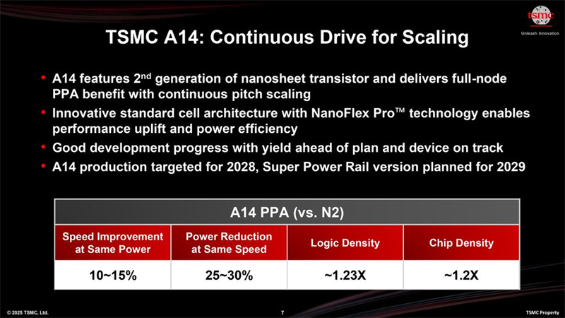
TSMC announced its next-generation A14 (1.4nm-class) process technology at its 2025 North American Technology Symposium on April 23, confirming plans to begin mass production in 2028. The A14 node, based on the company's second-generation gate-all-around (GAA) nanosheet transistors and enhanced NanoFlex Pro design architecture, promises up to 15% speed improvement or 30% power reduction over the upcoming N2 node, with at least 20% higher logic density.
Kevin Zhang, TSMC's Senior Vice President of Business Development and Global Sales, described A14 as a “full-node” leap beyond N2, offering enhanced performance and flexibility for AI and edge computing applications. The initial A14 version will not include backside power delivery, though a follow-up version featuring this enhancement is scheduled for 2029.
A highlight of A14 is its NanoFlex Pro technology, which supports design-technology co-optimization (DTCO) and allows chipmakers to fine-tune power, performance, and area (PPA) tradeoffs more precisely. A14 will require new IPs and design tool flows, distinguishing it from N2P and the future A16 node.
TSMC Chairman and CEO C.C. Wei emphasized that A14 will play a key role in driving AI innovation across devices, stating, “Our customers are always looking forward, and TSMC's technology leadership provides a trusted blueprint for innovation.” The symposium, attended by over 2,500 participants, also featured an Innovation Zone showcasing products from startup customers.
Alongside A14, TSMC revealed progress across its technology platforms, including logic, specialty, advanced packaging, and 3D integration:
● Advanced Packaging & HPC: TSMC is ramping up its CoWoS (Chip-on-Wafer-on-Substrate) packaging technology to support AI workloads requiring massive logic and high-bandwidth memory (HBM) integration. A next-gen SoW-X platform, boasting 40x the compute capacity of existing CoWoS, is slated for production in 2027.
● Mobile: The N4C RF process, scheduled for risk production in Q1 2026, targets edge AI connectivity with 30% lower power and area compared to N6RF+, supporting emerging standards like WiFi 8 and AI-enhanced wireless earbuds.
● Automotive: TSMC's N3A node is nearing completion of AEC-Q100 qualification and is tailored for advanced driver-assistance systems (ADAS) and autonomous vehicles, balancing performance with automotive-grade reliability.
● IoT: For ultra-low-power edge AI, TSMC is scaling its N6e and upcoming N4e nodes to extend energy efficiency.
In the near term, TSMC is also advancing its 3nm family. The performance-optimized N3P node has officially entered mass production, offering 5% higher performance or 5–10% lower power than N3E, along with up to 4% greater transistor density. It retains full IP compatibility and is well-suited for designs with heavy SRAM usage.
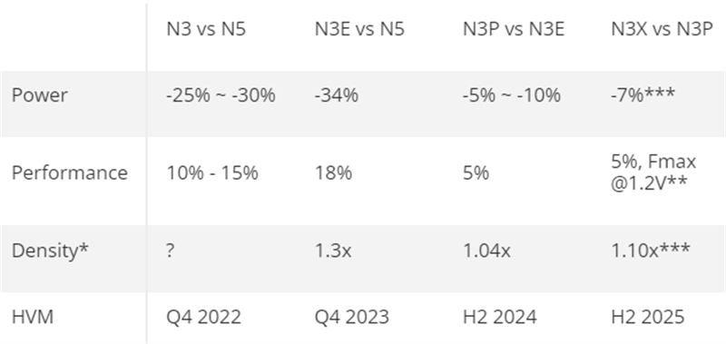
The next in line, N3X, is scheduled for production in the second half of 2025. It delivers a further 5% performance uplift or 7% power savings over N3P and supports voltages up to 1.2V — crucial for applications pushing frequency limits, such as high-end CPUs. However, the elevated voltage also increases leakage power, requiring careful design considerations.
TSMC reaffirmed its strategy of iteratively enhancing each node post-launch, as seen with the N5/N4 series, to maximize IP reuse and customer investment. While the industry eyes 2nm, TSMC expects many flagship client processors — including those powering the next-gen iPhone, iPad, and Mac — to continue leveraging the maturing 3nm platform.
+86 191 9627 2716
+86 181 7379 0595
8:30 a.m. to 5:30 p.m., Monday to Friday

