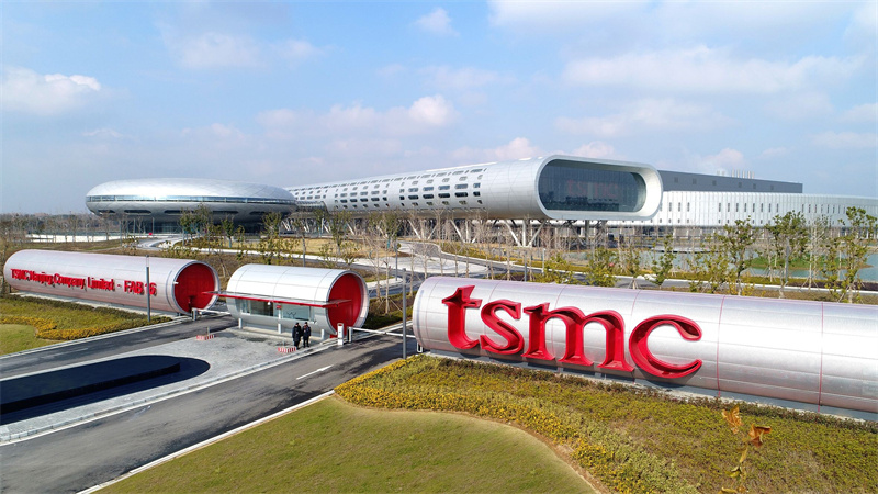
Taiwan Semiconductor Manufacturing Company (TSMC) is accelerating its rollout of 2nm production, with four fabs in Taiwan expected to reach a combined monthly capacity of 60,000 wafers by 2025. The company has already entered mass production at its first 2nm fab (P1) in Kaohsiung's Nanzi Science Park, with output reaching 10,000 wafers per month. A second fab (P2) in the same complex is undergoing equipment installation and is expected to begin pilot production by the end of 2024.
TSMC held a topping-out ceremony for the P2 fab in March and has since fast-tracked cleanroom construction and facility engineering. Once operational, the P1 and P2 fabs in Kaohsiung are expected to contribute up to 30,000 wafers per month. Construction is also underway on a third fab (P3), which will support the advanced A16 process node, with P4 and P5 in early development stages.
In northern Taiwan, TSMC's Baoshan (Hsinchu) F20 site is also preparing for large-scale 2nm production. The P1 line has completed risk ramp testing and started volume production, while the P2 fab has finished equipment installation. These two fabs are projected to contribute an additional 30,000–35,000 wafers per month by year-end.
All four fabs will use TSMC's next-generation nanosheet transistor architecture—similar to gate-all-around (GAA)—which offers up to 35% power savings or 15% performance gains compared to the company's 3nm node, along with 1.15x higher transistor density.

According to reports, trial yields for TSMC's 2nm process have reached around 60–65%, surpassing competing nodes like Intel 18A and Samsung SF2. While TSMC has not disclosed official yield figures, it has stated performance is better than expected.
Despite the production ramp, TSMC reportedly has no plans to offer discounts for its 2nm wafers, which are expected to cost approximately $30,000 each—50% more than 3nm. To help customers manage costs, TSMC launched a “CyberShuttle” service in April, allowing multiple clients, including Apple, to test designs on shared wafers.
TSMC believes 2nm and its A16 variant will be critical enablers for the next wave of AI and high-performance computing chips. It also plans to offer enhanced versions such as N2P, providing more options for smartphone and HPC customers.
The company revealed that design activity for 2nm is already outpacing 3nm and 5nm at the same stage, with nearly all major innovators onboard. Over the next five years, TSMC expects its 2nm platform to power up to $2.5 trillion in global end-product value.
Meanwhile, its 3nm node continues to mature, entering its third year of production with several variants (N3E, N3P, N3X). 3nm now accounts for 24% of TSMC's Q2 2025 revenue—approximately NT$224 billion—with further growth expected in the second half of the year. Analysts expect the 2nm production curve to closely mirror the successful ramp of 3nm.
+86 191 9627 2716
+86 181 7379 0595
8:30 a.m. to 5:30 p.m., Monday to Friday
