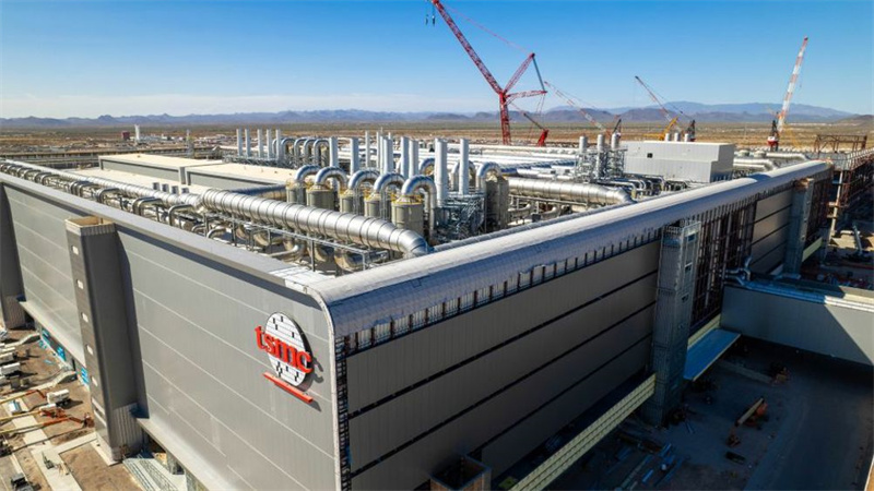
TSMC is ramping up its U.S. production plans and prices as American tech giants flood its Arizona fabs with chip orders in a bid to bypass looming semiconductor tariffs. The Taiwanese chipmaker is reportedly planning a 30% price hike at its U.S. facilities to cope with skyrocketing demand and offset high operational costs.
According to sources cited by Digitimes and Economic Daily, Apple, AMD, and NVIDIA are aggressively expanding their orders at TSMC's Arizona-based fab due to anticipated tariff hikes driven by the Trump administration's trade policies. The influx of orders has created a bottleneck at the company's 4nm production lines, prompting clients to compete for limited capacity.
To address this surge, TSMC is expected to raise its U.S. contract manufacturing prices by up to 30%. The move aims to mitigate the high cost of producing chips domestically and reduce the financial strain from its American operations.
In response to strong demand, TSMC is also accelerating its U.S. manufacturing roadmap. Its second Arizona fab, originally slated to begin equipment installation in Q4 2026, will now move that timeline up by a full year. Suppliers have reportedly been notified to deliver equipment as early as September 2025, with 3nm production targeted by the end of 2027. The second-phase line, set to produce 2nm chips, is expected to start in 2028—still two years behind Taiwan's schedule.
NVIDIA recently announced that its new 4nm Blackwell AI chips are already in production at TSMC's Arizona fab. The company is working with partners such as Amkor and ASE for back-end packaging and testing. AMD also confirmed on April 15 that its fifth-generation EPYC server processors are being produced in Arizona, with its upcoming 2nm Venice chips already taped out and planned for launch next year.
AMD CEO Lisa Su said the company plans to expand U.S.-based production of AI server chips to meet increasing domestic demand.
However, TSMC still faces a packaging bottleneck in the U.S. Currently reliant on a partnership with Amkor, the company has committed an additional $100 billion investment in the U.S., which includes two advanced packaging plants.
One of the key innovations TSMC plans to introduce in these facilities is fan-out panel-level packaging (FOPLP), a next-gen technology aimed at improving heat dissipation and substrate efficiency. Unlike traditional wafer-based methods, FOPLP arranges diced chips on a glass panel substrate. Though slower to produce than 3D stacking methods like CoWoS or SoIC, the glass-based approach is expected to appeal to AI hardware clients for its thermal advantages.

Japanese reports say TSMC will adopt a 300mm x 300mm FOPLP format for initial trial runs, set to begin as early as 2027 at a pilot line under construction in Taoyuan. The company had considered collaborating with panel makers like Innolux but opted for in-house development due to precision and technical challenges in adapting display industry methods to advanced chip packaging.
Meanwhile, U.S.-based EMS giants like Foxconn (Houston) and Wistron (Dallas) are preparing to mass-produce AI servers over the next 12–15 months. Industry analysts expect NVIDIA alone to help drive the production of up to $500 billion worth of AI infrastructure in the U.S. over the next four years.
With demand heating up and geopolitics reshaping the semiconductor landscape, TSMC is betting big on its U.S. expansion—even if it comes at a premium.
+86 191 9627 2716
+86 181 7379 0595
8:30 a.m. to 5:30 p.m., Monday to Friday

