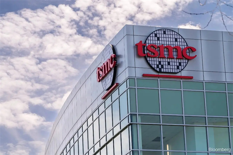
TSMC has confirmed plans to exit the gallium nitride (GaN) foundry business within two years, shutting down its 6-inch Fab 2 in Hsinchu Science Park, Taiwan. The company will also consolidate its three 8-inch fabs—Fab 3, Fab 5, and Fab 8—and reassign up to 30% of employees to facilities in the Southern Taiwan Science Park (STSP) and Kaohsiung. The move aims to ease labor shortages, cut costs, and optimize asset utilization.
Industry sources report that TSMC has mapped out new uses for its legacy fabs. The 6-inch plant will be repurposed as a CoPoS panel-level packaging facility, while the 8-inch fabs will pivot toward in-house production of EUV pellicles to reduce reliance on ASML and its supply chain. Fab 3 in Hsinchu will become the company's R&D hub for EUV pellicle technology.
The strategy reflects TSMC's push to leverage its R&D and manufacturing strengths to enhance EUV yields while controlling costs. EUV lithography is critical for sub-7nm nodes but comes with steep expenses—ASML's EUV scanners cost about $150 million each, while its next-generation High-NA EUV systems exceed $350 million. TSMC has cut back on High-NA orders and is focusing on yield improvements through pellicle innovation.

Pellicles are essential for protecting EUV masks from particle contamination. Traditional organic pellicles lack the transparency and durability required for EUV, forcing most fabs to operate without them and conduct frequent inspections, raising defect risks and costs. While ASML and others are developing solutions, progress has been slow due to high technical barriers. TSMC believes EUV pellicles are critical for advanced nodes and is accelerating internal development.
Analysts suggest TSMC's self-developed pellicles could streamline workflows, improve yields, expand capacity, and reduce costs—strengthening its profitability and competitive lead. Although IP issues around pellicle technology remain unresolved, the shift is expected to generate new demand for equipment and materials across the supply chain.
The restructuring comes as TSMC scales CoWoS advanced packaging and prepares for sub-2nm production. Since early 2025, the company has been optimizing legacy fabs, including the sale of $71–73 million in equipment to Vanguard International Semiconductor (VIS) and VSMC, a joint venture with NXP in Singapore.
TSMC's withdrawal from GaN foundry services also highlights the intensifying price competition from mainland Chinese rivals in third-generation semiconductors. Global IDMs such as Texas Instruments and Infineon are ramping in-house GaN capacity, while Renesas has partnered with Polar Semiconductor on next-generation GaN development.
+86 191 9627 2716
+86 181 7379 0595
8:30 a.m. to 5:30 p.m., Monday to Friday
