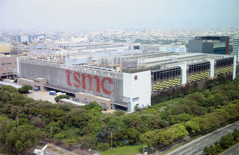
TSMC is moving ahead of schedule on its 1.4-nanometer process, with construction of a new fab at the Central Taiwan Science Park (CTSP) expected to begin in October, industry sources confirmed. The project, known as Fab 25, will ultimately include four plants, with the first set to begin risk production by late 2027 and mass production in the second half of 2028.
The CTSP Administration said water and soil conservation work for the second-phase expansion will be completed by the end of September, clearing the way for groundbreaking. Local suppliers, including cement, construction, and electromechanical firms, have already received tender notices, with total related business opportunities estimated at more than NT$3 billion (US$98 million).
According to TSMC's previously disclosed site plans, the Taichung facility will serve as the primary hub for its A14 (1.4nm) technology. The company intends to build four fabs in phases, with the first two dedicated to 1.4nm production. The second phase may advance further to A10 (1nm). Industry sources also indicated that TSMC has notified equipment vendors to prepare tools required for 1.4nm pilot lines, with installations expected at Hsinchu's Fab 20 later this year.

At its North America Technology Symposium in April, TSMC detailed the A14 node, based on its second-generation nanosheet gate-all-around (GAA) transistor and a new NanoFlex Pro standard cell architecture. Compared with N2, A14 is designed to deliver up to 15% higher performance or 30% lower power at the same speed, along with more than 20% greater logic density.
Kevin Zhang, TSMC's senior vice president of business development and deputy COO, described A14 as "our next full-node advancement," adding that it enables higher performance and energy efficiency while offering customers more design flexibility. TSMC is also planning enhanced versions—A14P with backside power delivery around 2029, followed by high-performance (A14X) and cost-optimized (A14C) variants.
The aggressive push comes as TSMC cements its dominance at the 2nm node. Mass production of 2nm chips is slated to ramp in Q4 2025 at Fab 20 in Hsinchu and Fab 22 in Kaohsiung, with monthly output expected to reach 50,000 wafers by year-end and exceed 100,000 wafers in 2026. Apple, AMD, Qualcomm, Broadcom, MediaTek, and Intel are among the first wave of 2nm customers, with NVIDIA, Amazon, and Google set to follow in 2027.
Rival foundries are struggling to keep pace. Intel's 18A process has reached a reported 55% yield, still trailing TSMC's 65% at 2nm. Samsung has postponed its own 1.4nm timeline from 2027 to 2029 as it focuses on improving 2nm yields, while Japan's Rapidus remains years behind in scale and commercial readiness.
With land already secured for an additional advanced node campus in Tainan's Shalun District, capable of supporting up to 10 fabs, TSMC is signaling its intent to maintain a decisive lead in the sub-2nm era.
+86 191 9627 2716
+86 181 7379 0595
8:30 a.m. to 5:30 p.m., Monday to Friday
