On November 5, 2025, TSMC began foundation construction on its A14 (1.4nm-class) manufacturing facility at the Central Taiwan Science Park in Taichung, according to reports from the Taiwan Economic Daily. The company did not hold a public groundbreaking ceremony, maintaining a low profile as it moves forward with tendering for subsequent construction phases. The total investment for the site is estimated at around NT$1.5 trillion (US$48.5 billion).
The new complex—designated as Fab 25—will eventually house up to four chip fabrication plants. The first fab is scheduled to complete risk production by late 2027 and begin mass production in 2028, with an initial monthly capacity of about 50,000 wafers. Once fully operational, the site could generate annual revenue exceeding NT$500 billion.
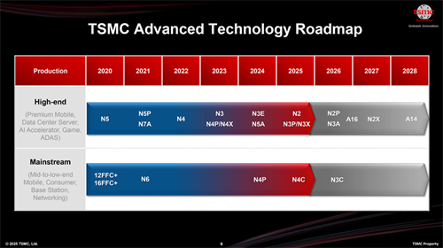
TSMC originally planned the Taichung site for 2nm production but later upgraded it to support 1.4nm or more advanced processes. The adjustment aligns with TSMC's strategy to maintain leading-edge manufacturing in Taiwan while distributing some 2nm production to overseas fabs, particularly in the United States, to mitigate geopolitical and supply chain risks.
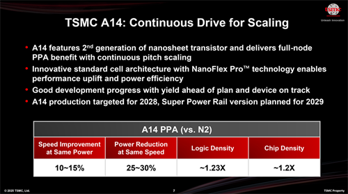
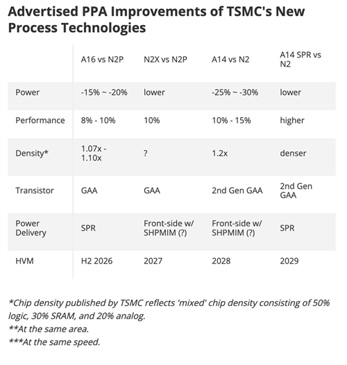
At the company's North America Technology Symposium earlier this year, TSMC outlined the technical roadmap for its A14 process, describing it as "a full-node advancement" over its N2 technology. The A14 process will use TSMC's second-generation gate-all-around (GAA) nanosheet transistors combined with NanoFlex Pro design technology to achieve up to 15% faster performance, 30% lower power consumption, and 20–23% higher transistor density compared with N2.
The first version of A14, expected to begin production in 2028, will not include backside power delivery (BSPDN). A subsequent version with backside power rails—tentatively called A14P—is planned for release in 2029, followed by higher-performance and cost-optimized variants (A14X and A14C).
TSMC Senior Vice President of Business Development and Co-Chief Operating Officer Kevin Zhang described A14 as "our next-generation, full-node silicon technology that sets a new benchmark in performance, power, and density." He noted that NanoFlex Pro enables greater flexibility in transistor design optimization, allowing chipmakers to tailor power-performance tradeoffs to specific workloads.

Unlike Intel's upcoming 14A process, which will adopt High-NA EUV lithography, TSMC's A14 will continue to rely on advanced multi-patterning techniques. Analysts say this reflects the company's confidence in its established EUV infrastructure and manufacturing expertise.
The A14 node is expected to serve both mobile and high-performance computing markets, with Apple, Qualcomm, and MediaTek among likely early adopters, alongside NVIDIA and AMD for next-generation AI chips.
Industry observers note that TSMC's expansion in Taichung is also reshaping the region's semiconductor ecosystem. The Central Taiwan Science Park, where TSMC is the anchor tenant, recorded NT$1.04 trillion in total revenue last year—81.7% of which came from integrated circuit manufacturing. The new fab is expected to further boost the park's annual semiconductor output beyond the NT$1 trillion mark as AI-driven demand for advanced chips continues to rise.
With construction now underway, the A14 fab cements TSMC's leadership in the global semiconductor race as it prepares to usher in the Angstrom era ahead of mass production in 2028.
+86 191 9627 2716
+86 181 7379 0595
8:30 a.m. to 5:30 p.m., Monday to Friday

