Synopsys, Cadence, and Siemens have each announced expanded partnerships with Samsung Foundry, securing major design tool and IP certifications across Samsung's most advanced semiconductor process technologies. The three EDA giants are collaborating with Samsung on multiple fronts—including 3DIC, AI, and low-power design—to enable next-generation chip innovation at nodes ranging from 14nm down to 2nm.
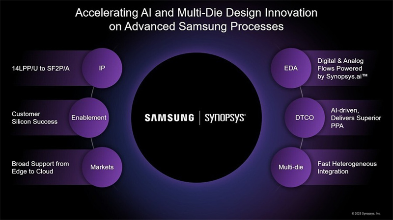
Synopsys Leads with 3DIC and AI Integration
Synopsys completed HBM3 tape-out using Samsung's SF2 process and I-CubeS packaging technology, achieving a 10x reduction in design cycle time and a 6% improvement in signal integrity. Its 3DIC Compiler has now been certified for the SF2P process, and the company has expanded its IP portfolio to support high-speed interfaces.
A Samsung Foundry design executive commented, “With Synopsys' 3DIC Compiler and IP portfolio, we're accelerating the realization of high-performance, low-power multi-die systems.”
Cadence Expands IP and AI-Driven Flow Across Multiple Nodes
Cadence signed a multi-year IP licensing agreement with Samsung, covering nodes from SF4X to SF2P. It has completed full digital flow certification for the SF2P node, and its AI tools have shown a 90% success rate in resolving IR-drop violations during CPU design. Cadence is also enabling migration of analog IP from 4nm to 2nm, supporting applications in AI data centers, automotive (including ADAS), and RF connectivity.
“Our comprehensive IP, subsystems, and chiplet solutions are enabling faster time-to-volume production for SoCs and 3DICs,” said a Cadence executive.
Siemens Deepens Joint Development with Samsung
Siemens EDA tools—including Calibre, Solido, and Aprisa—have been certified for Samsung Foundry's 14nm to 2nm process technologies, including FinFET and MCBFET nodes (SF2/SF2P). The companies are co-developing solutions targeting power integrity, silicon photonics, and analog/mixed-signal reliability.
A Samsung Foundry PDK leader stated, “Siemens continues to deliver functional enhancements for our ecosystem. Our collaboration extends beyond certification into co-developing differentiated EDA solutions.”
This multi-vendor engagement highlights Samsung's strategic push toward enabling chip designs for AI, 3D packaging, and high-performance computing, while reinforcing each EDA partner's influence in shaping the next wave of semiconductor innovation.
+86 191 9627 2716
+86 181 7379 0595
8:30 a.m. to 5:30 p.m., Monday to Friday

