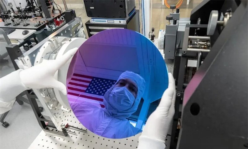
San Francisco-based startup Substrate announced on October 28 that it has developed an X-ray lithography (XRL) system that it claims can rival— and eventually surpass—ASML's most advanced High-NA EUV scanners, which cost nearly USD 400 million per unit. The company says its technology could reduce the cost of producing leading-edge silicon wafers from a projected USD 100,000 to around USD 10,000 by the end of the decade.
Founded in 2022 by brothers James and Oliver Proud, Substrate is developing a particle-accelerator-driven X-ray light source capable of printing 2 nm-class features and beyond. The company does not plan to sell lithography tools. Instead, it intends to build its own fabs in the United States and offer contract manufacturing services—a strategy that would require tens of billions of dollars and a new supply chain built from scratch.
A New Approach to Break the Cost Barrier
As chip features continue to shrink, the cost of lithography equipment has soared. ASML's current EUV systems sell for around USD 235 million, while its upcoming High-NA EUV scanners are approaching USD 380 million. Analysts estimate that a leading-edge fab will cost over USD 50 billion by 2030, pushing wafer prices toward USD 100,000 and limiting advanced chip production to only a handful of companies with massive capital.
Substrate argues this model is unsustainable. "By the end of the decade, Substrate will produce wafers closer to USD 10,000, not USD 100,000," the company stated on its website. CEO James Proud told Reuters he wants to build a cost structure that allows U.S. companies to compete with Asian semiconductor giants.
How X-Ray Lithography Works
Unlike ASML's systems, which rely on 13.5 nm extreme ultraviolet (EUV) light, Substrate uses short-wavelength X-rays generated by a custom-built particle accelerator. Electrons are accelerated to near light speed using radio-frequency cavities, then passed through alternating magnetic fields to produce ultra-bright bursts of coherent X-ray light—"billions of times brighter than the sun," according to the company.
These X-ray pulses are directed through ultra-polished grazing-incidence optics onto silicon wafers. Substrate has demonstrated 12 nm contact arrays with 13 nm tip-to-tip spacing and 30 nm-pitch vias, which—if achieved in real hardware—would outperform current Low-NA EUV scanners in critical dimension resolution and tip-to-tip fidelity.
However, the company has not revealed detailed information about resist materials, reticle technology, or throughput. Analysts note that current photoresists are incompatible with X-ray photon energies, meaning entirely new resist and mask technologies will need to be developed.
 and 13nm tip-to-tip (T2T) spacing printed with high pattern fidelity")

Massive Challenges Ahead
Despite promising laboratory data, Substrate still faces multiple engineering and commercial hurdles:
● Resist and optics development: Existing EUV resists cannot withstand high-energy X-rays, and large-scale production of grazing-incidence X-ray mirrors does not yet exist.
● Overlay and throughput: Substrate claims sub-1.6 nm overlay accuracy and 0.25 nm critical dimension uniformity in lab tests, but commercial-scale overlay of below 1 nm and high wafer-per-hour throughput remain unproven.
● Fab construction: The company plans to build its own vertically integrated fabs in the U.S. and is in talks with Texas A&M University about a USD 10 billion accelerator and manufacturing site.
● Supply chain gap: Unlike EUV, there is no existing infrastructure for X-ray-compatible masks, pellicles, metrology tools, or handling systems.
Substrate has raised over USD 100 million from investors including Founders Fund, General Catalyst, Valor Equity Partners and Peter Thiel, pushing its valuation above USD 1 billion. The team has grown to around 50 members, including engineers from TSMC, IBM and Google.

Strategic and Geopolitical Implications
Proud says he hopes to reduce America's reliance on overseas chipmakers such as TSMC and Samsung. U.S. officials have shown interest, though the company has not yet received direct federal funding. Analysts compare Substrate's ambitions to SpaceX—arguing that if chip manufacturing costs fall dramatically, it could unlock a new wave of innovation in AI, robotics and high-performance computing.
Yet investors and researchers caution that no X-ray lithography system has ever reached mass production. ASML's EUV journey—from its first prototype in 2006 to high-volume manufacturing in 2018—took over a decade and billions of dollars of ecosystem investment.
Still, Substrate claims its technology can achieve commercial production by 2028, positioning the U.S. to regain leadership in advanced semiconductor manufacturing. "The only way for America to lead again is to build a new kind of vertically integrated foundry that pushes Moore's Law further in performance and cost," the company said.
+86 191 9627 2716
+86 181 7379 0595
8:30 a.m. to 5:30 p.m., Monday to Friday

