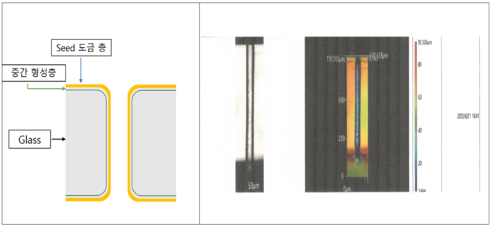
South Korea's DK Consortium has developed a new technology to overcome one of the toughest hurdles in mass-producing semiconductor glass substrates—the plating of through-glass vias (TGVs). By introducing an innovative "intermediate formation layer," the consortium is now moving into commercialization.
The DK Consortium, formed two years ago by Daichi Korea (a subsidiary of Japan's Daichi), DK Solution, and Aculaser, announced that the technology enables stable plating and metallization on TGV holes, a critical step in next-generation substrate manufacturing. Glass substrates, seen as a promising option for advanced semiconductor packaging, require thousands of microscopic TGV holes to be drilled and uniformly filled with copper or other metals to transmit electrical signals. Achieving consistent filling without defects has been a major bottleneck.
The newly developed ultra-thin intermediate layer coats the glass surface, allowing metal plating to adhere more uniformly and improving bond strength and process stability. According to the consortium, the technology has been applied to 510×515 mm glass substrate panels and has already completed commercialization of related liquid materials, coating methods, and deposition equipment.

With this breakthrough, the consortium has officially entered the semiconductor glass substrate process business. Member companies plan to jointly provide core steps such as TGV drilling, plating and metallization, and substrate dicing. They have previously demonstrated TGV holes with an aspect ratio of 150:1 and are now completing final reliability and quality evaluations with global semiconductor customers.
Daichi Korea will oversee collaboration with the Japanese parent company on bonding and film materials, DK Solution will handle sales and distribution, and Aculaser will lead equipment and process development for laser drilling, glass core substrate cutting, and package bonding.

Looking ahead, DK Consortium plans to develop new solutions enabling direct plating on TGV holes under 50 μm by next year, while also considering localized production of materials and small-volume manufacturing (SVM) of up to 1,000 glass substrates per month in South Korea.
A consortium representative said: "We can now provide a total solution covering TGV formation, metallization, key materials, and processing equipment. We are also preparing evaluations with domestic glass substrate manufacturers."
+86 191 9627 2716
+86 181 7379 0595
8:30 a.m. to 5:30 p.m., Monday to Friday
