SEMI on June 25 released its latest 300mm Fab Outlook report, projecting strong momentum in global semiconductor manufacturing. From late 2024 to 2028, global 300mm fab capacity is expected to grow at a compound annual growth rate (CAGR) of 7%, reaching a record 11.1 million wafers per month (wpm).
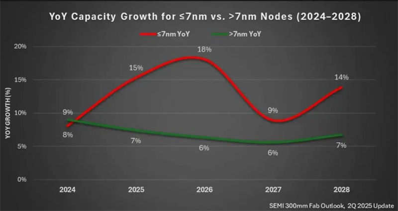
The primary driver of this growth is the continued expansion of advanced process capacity (7nm and below), which is set to rise 69% from 850,000 wpm in 2024 to a record 1.4 million wpm in 2028. This represents a CAGR of 14% – double the industry average. SEMI forecasts that advanced node capacity will reach a major milestone in 2026, surpassing 1 million wpm for the first time and hitting 1.16 million wpm.
Capacity for nodes at 2nm and below is expected to see especially aggressive expansion, climbing from under 200,000 wpm in 2025 to over 500,000 wpm by 2028. This reflects strong market demand driven by AI applications in advanced manufacturing.
"AI continues to be a transformative force across the global semiconductor industry, fueling rapid expansion of advanced manufacturing capacity," said Ajit Manocha, President and CEO of SEMI. "Its accelerating adoption is spurring investment across the entire semiconductor ecosystem, underscoring the industry's vital role in meeting the growing demand for advanced chips."
Equipment Spending for Advanced Nodes to Surge Through 2028
SEMI also noted that industry investment remains firmly focused on advanced node technologies. Capital spending on equipment for advanced nodes is expected to soar to over $50 billion in 2028, nearly doubling from $26 billion in 2024. This represents a robust CAGR of 18%.
The shift toward cutting-edge nodes is intensifying, with 2nm mass production expected in 2026 and commercial deployment of 1.4nm technology anticipated by 2028. To meet growing demand, chipmakers are proactively expanding capacity, with annual growth rates of 33% and 21% forecast for 2025 and 2027, respectively.
Investment in equipment for 2nm and below is particularly notable, expected to more than double from $19 billion in 2024 to $43 billion in 2028—a staggering 120% increase.
$400 Billion in Global 300mm Fab Equipment Spending Expected from 2025 to 2027
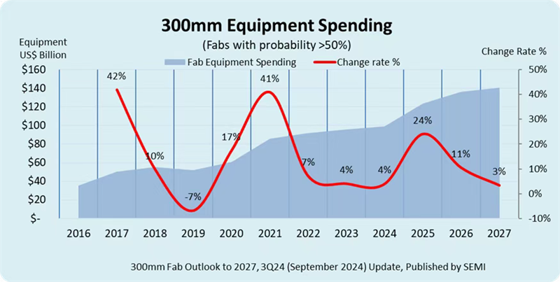
According to an earlier SEMI report, global spending on 300mm fab equipment is projected to hit a record $400 billion between 2025 and 2027. This surge is driven by the regionalization of semiconductor fabs and rising demand for AI chips in data centers and edge devices.
Chipmakers are expected to spend around $230 billion on equipment during this period, primarily for advanced nodes and sustained investments in mature processes. Key technologies at advanced nodes include 2nm process development, gate-all-around (GAA) transistor architecture, and backside power delivery.
At mature nodes, 22nm and 28nm processes are set to grow, supported by increased demand in automotive electronics and IoT applications.

The logic and microprocessor segments are expected to lead in equipment investment over the next three years with $173 billion in spending. Memory follows with over $120 billion, including more than $75 billion for DRAM-related tools and $45 billion for 3D NAND.
Power semiconductors rank third with over $30 billion in expected investment, including approximately $14 billion for compound semiconductor projects. Analog/mixed signal and opto/sensor categories follow with projected investments of $23 billion and $12.8 billion, respectively.
+86 191 9627 2716
+86 181 7379 0595
8:30 a.m. to 5:30 p.m., Monday to Friday

