South Korea-based inspection equipment company SEC will acquire electron beam (e-beam) based Through-Glass Via (TGV) processing technology from the Korea Institute of Industrial Technology (KITECH), marking a strategic expansion into the semiconductor manufacturing equipment sector.
SEC announced it has signed a five-year, five-month technology transfer agreement with KITECH to obtain high-voltage e-beam system design and manufacturing technology for TGV drilling. The deal includes a fixed technology fee of KRW 500 million (approx. USD 360,000) and royalties of 2.5% of sales generated from the technology—capped at KRW 1 billion—if revenue is generated over the next decade.
While SEC has so far applied its e-beam technology mainly in industrial inspection systems, the company now aims to enter broader markets including semiconductor fabrication, healthcare, security, defense, and sterilization. The newly transferred technology will be used to develop an e-beam-based TGV processing system for glass substrates, which are increasingly seen as essential for next-gen AI semiconductors.
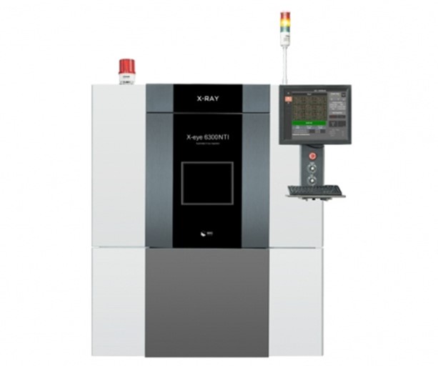
Last year, SEC delivered a manual X-ray inspection system for TGVs to JNTC and is targeting orders for inline equipment in the second half of 2025. If successful, SEC will offer both TGV processing and post-Cu-fill inspection tools—positioning itself across the full process flow.
The transferred e-beam drilling technology, a subset of the $3.9 billion global electron beam machining (EBM) market, has traditionally been used in high-precision fields such as aerospace, nuclear, and defense. Its application in semiconductors, particularly for glass substrates and silicon wafer interposers, remains at an early stage, but KITECH's solution is said to be highly refined after a decade of R&D focused on micro-hole drilling.
SEC plans to combine this with its own proprietary e-beam technology and expects to commercialize the system as early as 2028. The global market for glass substrates is projected to grow from $240 million this year to $1.13 billion by 2055, with a CAGR of 29.5%—making TGV e-beam drilling a potential future growth driver.
Compared to traditional laser-based TGV processes, e-beam drilling offers several advantages. Laser methods often require complex chemical etching, while e-beam enables high-precision hole formation without additional chemicals—reducing production costs in semiconductor packaging.
Additionally, e-beam technology can drill micro-scale holes with aspect ratios exceeding 10:1, which is advantageous for high-density, high-integration next-generation semiconductor packages.
An SEC spokesperson emphasized the broader potential of EBM: “Beyond drilling, e-beam technology plays a key role in precision fields such as e-beam welding and semiconductor lithography. However, Korea still relies entirely on imports. Starting with the development of TGV drilling systems, we aim to localize e-beam welding and lithography equipment by leveraging our existing technologies like X-ray and scanning electron microscopy (SEM).”
+86 191 9627 2716
+86 181 7379 0595
8:30 a.m. to 5:30 p.m., Monday to Friday

