Samsung Electronics plans to adopt glass substrate-based advanced semiconductor packaging technology by 2028, marking a major strategic shift aimed at strengthening its competitiveness in high-performance AI chips.
According to industry sources on May 26, Samsung has finalized a roadmap to replace traditional silicon interposers with glass interposers, a move that positions the company alongside global leaders such as AMD and Intel, who are also eyeing commercialization of glass substrates around the same time.
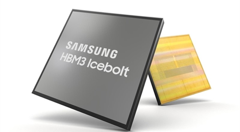
Glass interposers offer key advantages in high-speed data processing, heat resistance, and durability—making them ideal for AI chips that require robust signal transmission between GPUs and high-bandwidth memory (HBM). While silicon has traditionally been the material of choice, its high cost and manufacturing complexity have become limiting factors, accelerating the industry's shift to glass-based solutions.
Samsung aims to maximize process efficiency by utilizing its panel-level packaging (PLP) lines at its Cheonan campus. The company is also in talks with suppliers to build a stable glass substrate supply chain and is evaluating unit-level application strategies tailored to specific chip sizes.
Industry insiders see the move as a response to soaring demand for AI semiconductors and part of Samsung's broader push to offer integrated AI solutions through its foundry, HBM, and system semiconductor operations.
News of Samsung's commitment to glass substrates has also ignited investor interest in related stocks. Shares of Ram Technology surged more than 17% on May 26, with other glass substrate-related firms such as P.I.E, Hanbit Laser, Philoptics, and YCC also posting strong gains.
Ram Technology is viewed as a key beneficiary due to its patent for glass hole etching technology used in Through Glass Via (TGV) interposers. The company is co-developing TGV etching solutions with Samsung Electro-Mechanics, targeting mass production in 2026.
Founded in 2001 and listed on KOSDAQ since 2013, Ram Technology supplies specialized etchants and chemical materials to major clients such as SK hynix and Samsung SDI, serving sectors including semiconductors, displays, secondary batteries, and solar cells. The company continues to expand globally through localized R&D and automated manufacturing to boost efficiency and profitability.
Industry analysts believe Samsung's adoption of glass substrates could serve as a catalyst for the broader transition toward next-generation semiconductor packaging, offering both performance gains and cost advantages.
+86 191 9627 2716
+86 181 7379 0595
8:30 a.m. to 5:30 p.m., Monday to Friday

