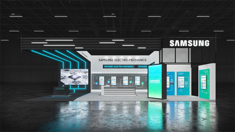
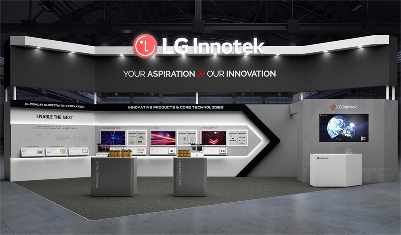
Samsung Electro-Mechanics (009150.KS) and LG Innotek (011070.KS) are highlighting their latest advances in next-generation package substrates at the KPCA Show 2025, held September 3–5 at Songdo Convensia in Incheon, South Korea. The annual event, now in its 22nd year, is the country's largest PCB and semiconductor packaging exhibition, bringing together more than 240 companies to showcase cutting-edge technologies.
Samsung Electro-Mechanics is accelerating development of glass core substrates, which are viewed as a key technology for future high-performance semiconductor packaging. The company said customer evaluations have confirmed that its glass substrates can reduce thickness while improving stability against heat and warpage, making them suitable for large-area, high-density applications.
Industry observers expect glass substrates to enter full-scale commercialization as early as 2027. Samsung Electro-Mechanics is working toward that timeline in cooperation with Samsung Electronics, focusing on developing a robust glass core insulation layer that reduces overall chip size and improves warpage control compared with conventional copper-clad laminates (CCLs). The company reported success in halving through-glass via (TGV) pitch compared with plated through-holes (PTH) in CCLs, enabling more flexible design. Test results showed that a 10-layer CCL design could be reduced to six layers using glass substrates without performance issues, while also cutting warpage by about 30% at room temperature and over 90% at high temperatures.

"By 2027–2028, package substrates will become significantly larger, and limitations of CCLs will increase," said Lee Seung-eun, Head of the Substrate Business at Samsung Electro-Mechanics, during the KPCA forum. "Glass substrates will emerge as a strong alternative, particularly for high-performance applications where multilayer cores are no longer sufficient."

Alongside glass substrates, Samsung Electro-Mechanics is also displaying a wide portfolio of advanced packaging solutions. These include server-grade flip-chip ball grid array (FC-BGA) substrates—which feature areas more than ten times larger and layer counts over three times higher than standard FC-BGAs—2.1D substrates that connect chips without silicon interposers, co-package substrates integrating SoCs and memory, ultra-thin core (UTC) substrates for AI laptops, automotive-grade FC-BGAs, embedded substrates with passive components, and flip-chip chip-scale packages (FC-CSPs) for smartphone processors.

LG Innotek, meanwhile, is unveiling its proprietary copper-post (Cu-Post) technology, which replaces traditional solder ball mounting by adding microscopic copper pillars topped with solder balls to connect substrates with motherboards. This approach reduces substrate size by up to 20%, improves heat dissipation, and allows for higher circuit density. The company is also showcasing large-area FC-BGA substrates for AI and data centers, multilayer core (MLC) technology to improve warpage and signal performance, and glass substrates targeted for mass production between 2027 and 2028.
Both companies are betting on glass core technology as the next leap in substrate innovation, driven by the growing demands of AI, cloud computing, and automotive electronics. According to MarketsandMarkets, the global glass substrate market is projected to grow at over 18% annually, expanding from $7.1 billion in 2023 to $8.4 billion by 2028.
+86 191 9627 2716
+86 181 7379 0595
8:30 a.m. to 5:30 p.m., Monday to Friday
