Samsung Electronics has delayed the launch of its $44 billion semiconductor fab in Taylor, Texas, as it struggles to secure customers and adapt to rapidly changing process node demands. Sources told Nikkei Asia that even if the plant is completed and equipped, production cannot begin due to insufficient demand, with the originally planned 4nm process no longer matching current market requirements.
Samsung began construction on the Taylor facility in 2022 with an initial investment of $17 billion. In 2024, the company expanded the project to $44 billion to include two advanced logic fabs (one targeting 4nm and the other 2nm nodes), an R&D center, and an advanced packaging plant focused on 3D high-bandwidth memory and 2.5D technologies. In exchange, Samsung secured up to $6.6 billion in direct subsidies under the U.S. CHIPS and Science Act.
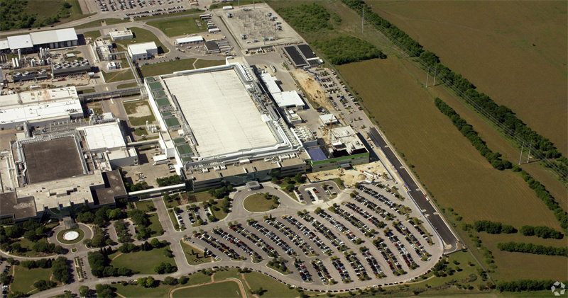
Internal documents revealed the site was 91.8% complete as of March 2024, with original plans for completion by April. That timeline was later revised to October. Despite construction progressing, Samsung has reportedly delayed equipment installation, which typically begins within three to six months after building completion.
The delay appears driven by lackluster demand from U.S. customers and limited interest in 4nm chips. A supply chain executive told Nikkei Asia that Samsung's planned process nodes are no longer aligned with market expectations, and any upgrade to the more competitive 2nm node would require a costly overhaul. For now, the company has adopted a wait-and-see approach.
In contrast, TSMC's Arizona-based Fab 21 has already begun mass production of 4nm chips and secured high-profile U.S. clients such as Apple, Nvidia, AMD, Broadcom, and Qualcomm. Despite higher production costs in the U.S., TSMC's capacity is reportedly sold out through 2027. TSMC currently leads the global foundry market with a 68% share, while Samsung ranks second with just 7.7%, according to TrendForce.
The situation underscores the challenges of setting up a cutting-edge chip fab in a new location. Beyond construction, Samsung must develop a local supply chain, recruit skilled talent, and win customer orders. Moreover, equipping the fab—particularly for 2nm node production—involves astronomical costs and complex technologies such as EUV lithography, etching, and advanced deposition.

Compounding the issue are global headwinds. Samsung continues to face weak demand in consumer electronics and NAND flash, persistent yield problems, and reduced capacity utilization due to U.S. export restrictions on advanced chips to China. The broader geopolitical landscape, including the U.S.-China tech conflict and tariffs on electronics, has further complicated Samsung's global strategy.
China's push for semiconductor self-sufficiency adds to the competitive pressure. Though still behind the U.S. in advanced process nodes, China's government-led efforts are driving rapid capacity growth, potentially making it the world's largest chip manufacturing base by 2030.
Despite these setbacks, Samsung insists it will bring the Taylor fab online by 2026. While it has not confirmed a specific timeline for equipment installation or customer engagement, industry observers note that Samsung must eventually begin operations in order to qualify for U.S. subsidies and avoid falling further behind TSMC.
For now, the Taylor project reflects the difficult balancing act facing global chipmakers: aligning massive long-term investments with fast-evolving technologies and shifting geopolitical dynamics.
+86 191 9627 2716
+86 181 7379 0595
8:30 a.m. to 5:30 p.m., Monday to Friday

