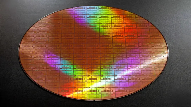
On July 18, Japan's Rapidus announced it has begun prototyping 2nm gate-all-around (GAA) transistor test wafers at its IIM-1 fab in Chitose, Hokkaido. The company confirmed that the early wafers are achieving expected electrical performance, signaling strong progress in its process development. This milestone marks Japan's official entry into next-generation logic foundry competition, joining the global ranks alongside TSMC, Samsung, and Intel.
Rapidus noted that the IIM-1 facility—under construction since September 2023—has rapidly matured. The cleanroom was completed in 2024, and more than 200 tools, including EUV and DUV lithography systems, were installed by June 2025. The company received its first EUV scanner from ASML in December 2024 and began initial exposures in April 2025. As of now, the fab is fully equipped for trial runs of 2nm chips.
Unlike traditional fabs, Rapidus is employing a full single-wafer processing model for all front-end steps, from oxidation and ion implantation to deposition and etching. This method allows for real-time, per-wafer process control, anomaly detection, and faster tuning, generating granular data that can feed AI algorithms for continuous improvement. Although more expensive and slower than batch processing, the company believes this approach will enhance defect reduction, yield, and long-term efficiency—particularly important for its focus on specialty chips.
The company expects to release its first Process Design Kit (PDK) in Q1 2026 to support customer design activities. It also announced collaboration with Siemens to develop a manufacturing-design co-optimization (MDCO) solution based on the Calibre platform, aimed at shortening tape-out times and boosting production readiness.

Rapidus's 2nm technology is based on nanosheet GAA transistors developed in collaboration with IBM. The company skipped directly from 40nm to 2nm—a bold leap supported by IBM's transistor architecture, EUV lithography know-how from Belgium's imec, and advanced nanoimprint technologies co-developed with Canon and Kioxia. IBM researchers say the process simplifies nanosheet transistor manufacturing compared to FinFET, easing scale-up for mass production.
CEO Atsuyoshi Koike has emphasized that Rapidus will not compete directly with TSMC in high-volume standard chip production. Instead, the company is targeting emerging markets such as robotics, autonomous driving, and remote healthcare. Broadcom is reportedly among its first customers, with 2nm chip samples delivered in June 2025. NVIDIA is also rumored to be considering Rapidus for future AI chip production, while Japanese firms like Preferred Networks and Sakura Internet are already lined up as partners.
With functional 2nm test wafers now in hand and its process pipeline advancing, Rapidus is positioning itself as a serious contender in the next era of logic chip manufacturing.
+86 191 9627 2716
+86 181 7379 0595
8:30 a.m. to 5:30 p.m., Monday to Friday

