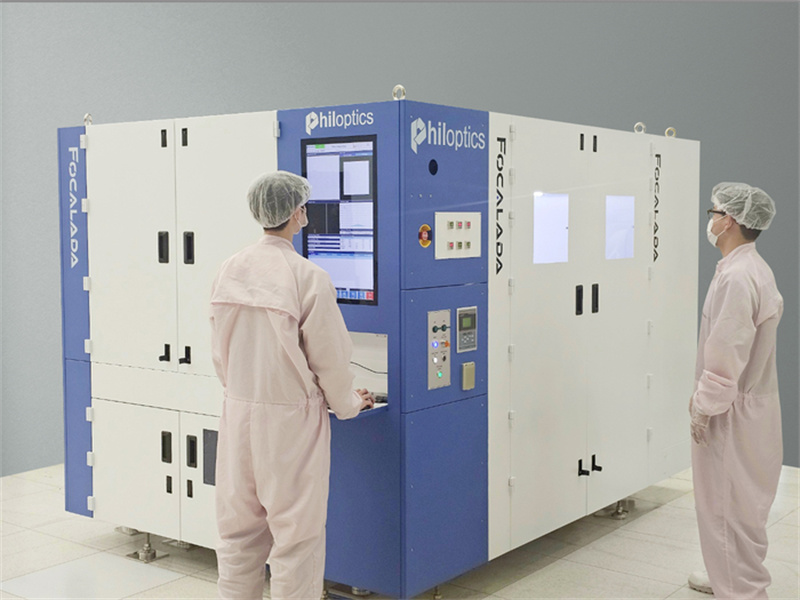
South Korean laser equipment maker Philoptics (KOSDAQ: 161580) has developed a new inspection system for Through Glass Via (TGV) holes in semiconductor glass substrates, the company announced on April 30. The equipment is designed to detect defects in hole shape, size, position, and potential damage to the substrate—key quality metrics in next-generation semiconductor packaging.
The inspection process involves sequential steps of high-speed imaging, scanning, image generation, and defect identification. Using an advanced optical system developed with SD Optics, the equipment can simultaneously capture the top, middle, and bottom sections of each TGV hole—up to 1.9 million per panel—within approximately 16 minutes. This full-surface imaging is enabled by a tilted camera approach that creates a 2.5D image, improving accuracy without flipping the substrate.
Philoptics applied deep learning and big data analytics to handle image files as large as 700GB per panel. This enables automated classification and analysis of defects, significantly improving inspection speed and production yield. The company emphasized that accurate and fast defect detection is a critical bottleneck in scaling glass substrate production for advanced packaging.
The new equipment expands Philoptics' semiconductor glass substrate portfolio to five product lines, which already include TGV drilling, Ajinomoto Build-up Film (ABF) drilling, direct imaging (DI) exposure systems, and singulation tools. The company has supplied these systems to major global customers, with additional shipments expected within this year.
Philoptics sees the inspection system as a strategic complement to its existing TGV drilling equipment, noting that customers increasingly demand integrated solutions for defect detection and process control. The company began TGV equipment development in 2019 and has since internalized key capabilities for production yield evaluation.

Philoptics is also targeting glass substrate R&D and metrology needs in the materials and components sectors, with discussions underway for both domestic and overseas supply. Initial deliveries of the inspection system are expected as early as Q3 or Q4 2025.
Notably, in March, Philoptics shipped its first laser singulation equipment to a global semiconductor customer—building on its earlier achievement as one of the first suppliers of TGV drilling tools for high-volume production lines.
“We aim to reshape the inspection landscape, which has long relied on slower measurement-based defect detection,” said Vice President Choi Woo-hyuk, who led the development. “With this new solution, we are responding to a surge in demand tied to the commercialization of glass-based semiconductor packaging.”
+86 191 9627 2716
+86 181 7379 0595
8:30 a.m. to 5:30 p.m., Monday to Friday

