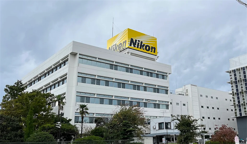
On August 21, Nikon announced it will permanently shut down its Yokohama Plant on September 30, a manufacturing site that has operated since 1967 and once stood as a symbol of Japan's rise in the global semiconductor industry. The closure marks the end of the company's golden era in lithography equipment manufacturing and underscores broader structural shifts in Japan's high-tech sector.
Nikon said operations and staff — about 350 employees as of July — will be transferred to newer, more automated facilities in Iwate and Miyagi prefectures, as well as other sites in Kanagawa. The company described the move as part of a long-term strategy to consolidate production, reduce costs, and adapt to changing market conditions. The one-time costs of closure, including employee relocation and asset write-downs, have been factored into its fiscal 2025 outlook. Nikon projects revenue for its Precision Equipment division will fall 8.4% year-on-year to JPY 185 billion (US$1.24 billion).
From Global Leader to Niche Player
The Yokohama Plant played a central role in Nikon's transformation into a global lithography powerhouse. In the 1980s and 1990s, Nikon and Canon dominated mid-range lithography systems, supplying giants such as IBM, Texas Instruments, Toshiba, and NEC. Even into the 2000s, Nikon remained a key competitor in i-line and KrF deep ultraviolet (DUV) equipment, forming a "big three" alongside ASML.
But as ASML's extreme ultraviolet (EUV) technology reshaped the industry, Nikon retreated to the mature-node market, where its tools remained widely deployed for power devices, display drivers, MCUs, and sensors, particularly in fabs across China and Southeast Asia.
Pressures Behind the Decision
Industry analysts cite several factors driving Nikon's retreat:
● Weak market demand: Global semiconductor inventory corrections have reduced appetite for mid- and low-end lithography systems, while display markets have stagnated.
● Customer setbacks: Intel, a long-standing key client, has delayed new fabs and cut capital spending, hitting Nikon's order pipeline.
● Geopolitical restrictions: Stricter U.S.-led export controls on equipment to China have raised compliance costs and delivery risks.
● Domestic challenges: Japan's high operating costs and aging workforce made the continued operation of Yokohama unsustainable compared with more automated northern plants.

New Strategic Focus
Despite the contraction, Nikon is repositioning toward growth niches. The company has entered advanced packaging, including fan-out wafer and panel-level lithography for chiplet and AI applications. In July, Nikon began taking orders for its DSP-100 digital lithography system, targeting 600 mm square panels for advanced packaging lines. Beyond semiconductors, the company is expanding in automotive optics, LiDAR, biomedical imaging, and space observation instruments.
A Broader Industry Shift
The closure also reflects the long decline of Japan's once-dominant semiconductor sector. In the 1980s, Japanese firms commanded nearly half of the global chip market. But U.S. trade pressure, the rise of Korean and Taiwanese competitors, and structural weaknesses eroded that lead. Today, advanced nodes are dominated by TSMC, Samsung, and Intel, while EUV lithography is monopolized by ASML.
Analysts say Japan is shifting from head-to-head competition toward specialized strengths in materials, equipment, and sensors. For Nikon, the shutdown of its 58-year-old Yokohama Plant symbolizes both the end of a golden chapter and the start of a more focused, niche-driven future.
+86 191 9627 2716
+86 181 7379 0595
8:30 a.m. to 5:30 p.m., Monday to Friday

