Two South Korean companies, AnyCasting and LaserApps, unveiled key innovations in glass substrate manufacturing this May, signaling steady progress in next-generation semiconductor packaging technologies.
AnyCasting Develops Void-Free Copper Plating for Glass Substrates
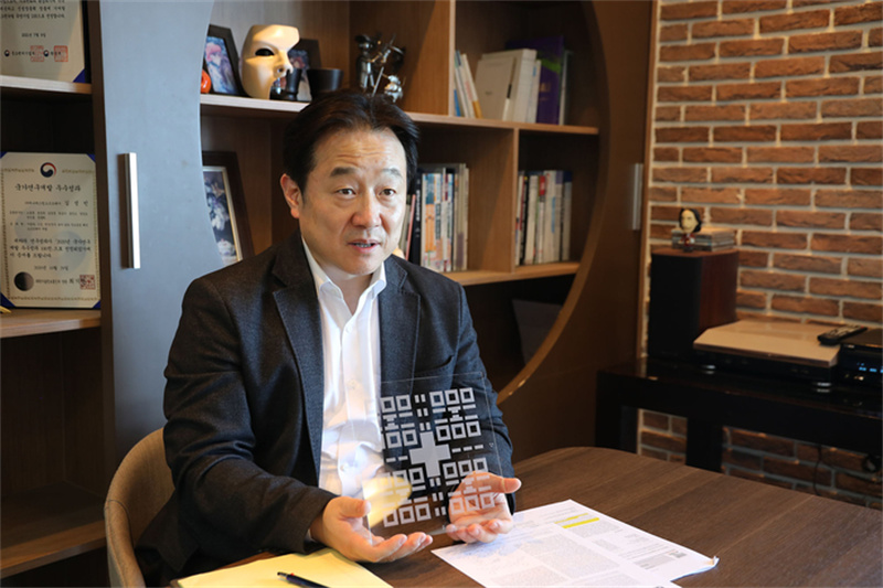
On May 11, AnyCasting announced it has developed a new copper plating technology for semiconductor glass substrates that eliminates voids inside Through-Glass Vias (TGVs). Company CEO Kim Sung-bin stated that their proprietary ion concentration control technology enables precise and uniform copper filling of TGVs, which are critical for electrical signal transmission in glass substrates.
Void formation during plating has long been a challenge, often compromising electrical and thermal performance. While the industry generally tolerates 1–3% voids by volume, AnyCasting emphasized that even small voids could threaten long-term reliability. The company claims to have achieved 0% voids using a 3D metal ion printing process.

In addition to developing its own plating equipment, AnyCasting is working with partners across the TGV ecosystem, including global glass material suppliers, laser etching specialists, and polishing equipment vendors. Kim noted that plating and polishing processes must be tightly integrated to ensure stable quality, particularly as substrate sizes increase. The firm is currently conducting multiple sample tests and aims to automate the entire glass substrate process, from cleaning to copper filling.
LaserApps Unveils Plasma Melting TGV Drilling Technology
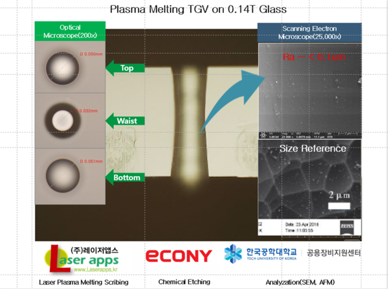
On May 8, LaserApps introduced a new laser-based drilling process that uses plasma melting to create precise TGV holes in glass substrates without cracks or internal defects. By generating controlled melting spots inside the glass, the method produces smooth, stable vias with improved electrical performance.
CEO Jeon Eun-sook explained that the condition of the TGV's inner walls directly impacts signal integrity and plating quality. The plasma melting technique helps minimize microcracks that could otherwise lead to substrate failure during downstream processing.
In collaboration with etching specialist Econy, LaserApps successfully formed 50µm TGV holes in 0.14mm-thick glass samples. The company also validated its results through analysis by the Korea Polytechnic University's shared equipment center.

Building on its earlier plasma laser cutting systems, LaserApps plans to commercialize this new drilling technology as part of its next growth engine. Patent filings have been submitted, and several semiconductor substrate manufacturers are already using LaserApps equipment for prototype production.
The company showcased the technology at the April “Tech Day: All About Semiconductor Glass Substrates” conference hosted by ETNews, where its presentation drew strong interest.
+86 191 9627 2716
+86 181 7379 0595
8:30 a.m. to 5:30 p.m., Monday to Friday
