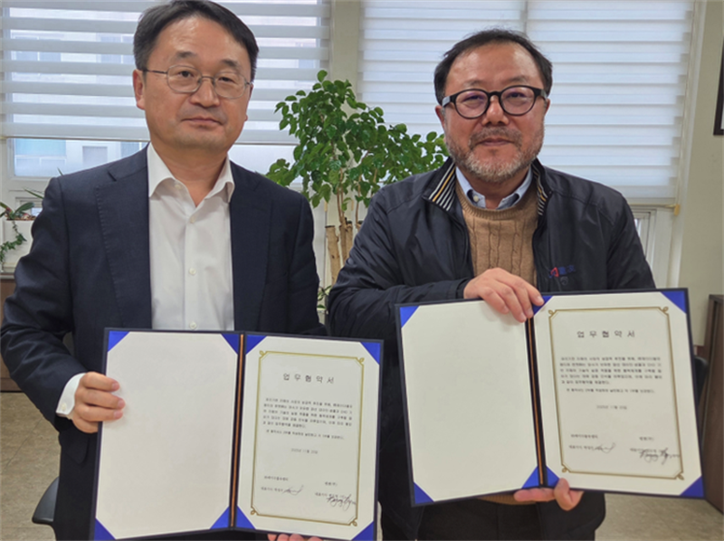
South Korea's emerging precision-printing equipment developer Enjet announced on November 24 that it signed a memorandum of understanding on November 21 with leading domestic glass substrate manufacturer JWMT (formerly JOONGWOO M-Tech) to jointly develop post-processing technologies for next-generation high-density glass substrates used in advanced semiconductor packaging.
Demand for glass substrates has surged as AI servers and high-performance semiconductor packages scale rapidly. The increased adoption of ultra-fine Through-Glass-Via (TGV) processes has made yield improvement and process stability major challenges for global manufacturers.
Today, glass substrate lines typically scrap an entire panel once defects are detected during inspection. As TGV dimensions shrink, plating and planarization become more complex, further weakening yields and raising production losses. Industry estimates suggest that even a 1% improvement in yield could translate into tens of billions of KRW in additional annual profitability, making a shift from defect rejection to defect repair an increasingly attractive alternative.
Under the collaboration, Enjet's high-precision electrohydrodynamic (EHD) micro-dispensing technology will be combined with JWMT's extensive glass substrate manufacturing expertise. The companies will evaluate the introduction of a new repair process that locally fills incomplete or defective TGV-related regions—areas that previously would have resulted in full-panel scrapping.
Both firms plan to advance the effort through on-site validation tests, after which they will assess commercial feasibility and phased integration into JWMT's production lines. If successfully adopted, the process could enhance substrate yields, improve ESG outcomes, and reduce operational expenses across the glass substrate value chain.

An industry official noted, "Global semiconductor leaders are all looking for ways to stabilize glass substrate post-processing, but this is effectively the first collaboration that aims to install a repair solution directly into production lines. It is highly meaningful because it offers a practical, domestically developed alternative for improving process yields."
Enjet added that, having supplied PCB SR-repair systems to global package substrate manufacturers earlier this year, it aims to leverage that experience to accelerate validation and move quickly toward commercialization of its glass-substrate repair technology.
+86 191 9627 2716
+86 181 7379 0595
8:30 a.m. to 5:30 p.m., Monday to Friday

