South Korean memory manufacturers continue to dominate the high-bandwidth memory (HBM) market, but they may be vulnerable in future technology transitions due to a lack of core patents in hybrid bonding, according to a recent report by Korean outlet TheElec.
Kim In-soo, a researcher at the Korea Intellectual Property Promotion Agency (KIPRO), said in an interview that although Korean chipmakers excel in HBM manufacturing and stacking—and collectively hold most of the global market—they rely heavily on overseas suppliers for materials and equipment, while holding relatively few high-value hybrid bonding patents. This could expose them to patent litigation in the future, he warned.
Data from Counterpoint Research shows that in the second quarter of this year, SK Hynix commanded 62% of the global HBM market, followed by Micron at 21% and Samsung Electronics at 17%. Together, SK Hynix and Samsung account for 79% of worldwide HBM shipments.
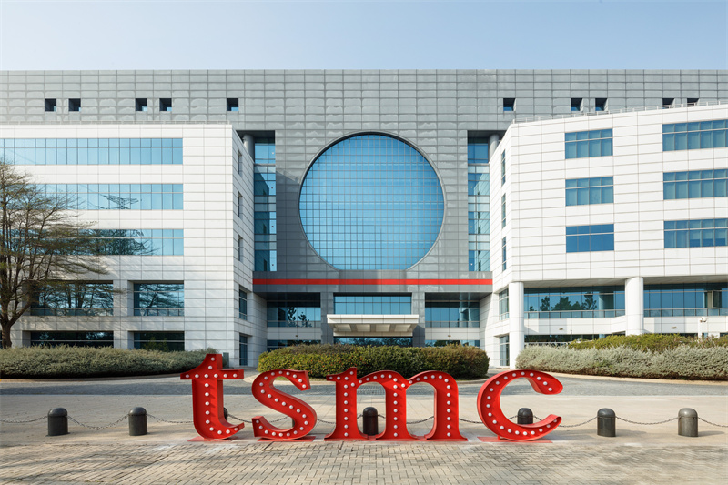
However, KIPRO’s analysis finds that the core hybrid bonding technologies essential for HBM manufacturing are led by U.S. company Adeia, Taiwan Semiconductor Manufacturing Company, and China’s Yangtze Memory Technologies Co. (YMTC).

Adeia, TSMC, and YMTC Hold the Most Valuable Patents
Kim said his research team used AI tools to review more than 10,000 patents related to hybrid bonding filed between 2003 and 2022 across Korea, the United States, Japan, Europe, and China. The study found that Adeia holds the most valuable hybrid bonding patents based on both quality and market relevance.
Adeia owns key low-temperature and direct-bond interconnect technologies originally acquired through Ziptronix. Its subsidiaries, including Invensas and Tessera, have built extensive patent portfolios covering hybrid bonding processes.
Based on the K-PEG patent quality rating, TSMC ranks first worldwide in the number of high-quality patents rated A3 or above, followed by Samsung, with Micron and IBM close behind. TSMC’s SoIC technology is also considered highly valuable in hybrid bonding applications.
China is rapidly expanding its patent presence in memory. YMTC holds core technologies such as its well-known Xtacking architecture, with patents registered across major jurisdictions including Korea, the United States, Japan, Europe, and China. This broad coverage increases the probability that Korean companies could face cross-border litigation.
A notable example of shifting IP dynamics occurred in February this year, when Samsung Electronics signed a patent licensing agreement with YMTC for hybrid bonding technologies required to develop over-400-layer NAND Flash. Samsung plans to apply YMTC’s hybrid bonding technology starting from its 10th-generation (V10) NAND products, which will reach 430 layers. Samsung reportedly concluded that it could not avoid YMTC’s patents for future high-layer NAND.
Hybrid Bonding Becomes Essential for 3D NAND and HBM
Hybrid bonding generally falls into two categories: wafer-to-wafer (W2W) and die-to-wafer (D2W). CBA-based NAND uses W2W hybrid bonding, eliminating traditional solder bumps and enabling sub-10-micron interconnect pitch. This shortens signal paths, increases I/O density, boosts data-transfer speeds, lowers power consumption, and reduces mechanical stress—significantly improving reliability.
As NAND stacking moves beyond 400 layers, the industry is shifting from a two-layer (array + CMOS) stack toward a three-layer structure: array + array + CMOS. This evolution further increases dependence on advanced hybrid bonding techniques.
Kim noted that while Korea possesses the second-largest number of HBM-related patents, their overall quality and influence are “below average.” Heavy reliance on imported materials and equipment adds further risk. Companies may continue to seek private licensing deals for now, but as hybrid bonding begins commercial adoption in 2026, unresolved IP issues could escalate into full-scale patent disputes.
+86 191 9627 2716
+86 181 7379 0595
8:30 a.m. to 5:30 p.m., Monday to Friday
