Japan's high-stakes bid to reinvigorate its domestic semiconductor sector is facing early setbacks. Despite announcing ¥9 trillion ($62 billion) in investments from 2022 to 2029—and over ¥10 trillion by fiscal 2030 to support AI and chip industries—only 3 of 7 factories built or acquired by Japanese companies in fiscal 2023 and 2024 have started mass production. The primary reason: sluggish demand for chips used outside of AI applications.
Renesas restarted its Kofu fab in April after nine years of dormancy, but postponed full production due to weak demand for power semiconductors in EVs and industrial systems. Rohm and Sanken Electric are similarly holding back on ramping up capacity, and Kioxia has delayed operations at its new memory plant until later this year. Even TSMC's new fab in Kumamoto—officially online since December 2024—is believed to be operating below capacity, with the launch of a second fab already postponed.
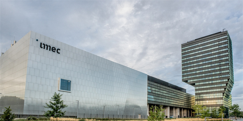
This domestic inertia contrasts sharply with the innovation-driven urgency elsewhere. In Belgium, imec—one of the world's leading semiconductor research institutions—is advocating a radical shift in chip design to meet the fast-moving demands of artificial intelligence. Ahead of its flagship ITF World conference in Antwerp, imec CEO Luc Van den hove issued a call for the industry to move beyond custom ASICs and embrace 3D-stacked, reconfigurable AI architectures.
Van den hove warned that the pace of AI algorithm development is far outstripping the hardware cycle. Custom chips can take 12 to 18 months to design and manufacture, by which time the software landscape may have already shifted—leaving expensive hardware obsolete. "There is a huge inherent risk of stranded assets," he said.
Instead, imec proposes a new architectural model: an array of programmable compute blocks called “supercells,” connected by a reconfigurable on-chip network. These supercells would enable chips to adapt in real time to evolving algorithmic needs—combining flexibility with performance. This approach requires true 3D stacking, integrating logic and memory across vertically bonded layers to optimize both compute density and energy efficiency.

While this idea shares DNA with FPGA concepts, imec's model operates at a higher abstraction level—leveraging heterogeneous compute units and rich memory arrays as building blocks. The goal: to balance performance, power, and area (PPA) more effectively in the face of AI's accelerating complexity.
Imec's track record lends weight to this vision. Over the past decades, the Leuven-based institute has played a central role in pioneering technologies now at the core of cutting-edge chipmaking, including FinFETs, gate-all-around transistors, backside power delivery, and advanced chiplet integration. Its research underpins upcoming nodes like TSMC's A14 and Intel's 18A-PT, both of which incorporate 3D stacking techniques developed in collaboration with imec.
As the AI frontier shifts from large language models to multimodal agentic systems in autonomous driving, robotics, and healthcare, Van den hove believes the semiconductor industry must adopt architectures that can evolve just as rapidly as the software they're meant to run.
While Japan continues to invest heavily in physical infrastructure, the question remains whether its fabs—many still focused on mature 12nm or 40nm processes—can align with this software-defined, AI-first future.
+86 191 9627 2716
+86 181 7379 0595
8:30 a.m. to 5:30 p.m., Monday to Friday

