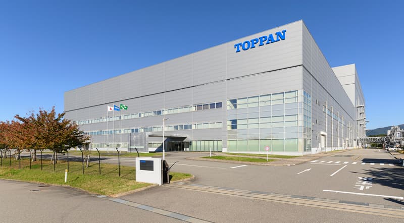
Recently, the diversified Japanese printing and electronics materials group TOPPAN Inc., a wholly owned subsidiary of TOPPAN Holdings Inc., announced plans to install a pilot line for advanced semiconductor packaging research and development at its Ishikawa Plant in Nomi, Ishikawa Prefecture. The site was acquired in 2023, and the pilot line is scheduled to be commissioned in July 2026.
The pilot line will focus on the development of organic redistribution layer interposers and other components essential for next-generation semiconductor packaging. The project has been selected for support under Japan's national Research and Development Project for Enhanced Infrastructures for Post-5G Information and Communication Systems, administered by the New Energy and Industrial Technology Development Organization. The initiative targets manufacturing technologies for advanced semiconductors.

As advanced semiconductors for applications such as generative AI and autonomous driving continue to evolve, packaging substrates are becoming larger and increasingly reliant on chiplet architectures. These architectures require interposers to electrically connect multiple chips to the packaging substrate. While silicon interposers remain dominant, limitations in scalability are accelerating industry interest in large-format glass-based interposers as an alternative.
Using the new pilot line, TOPPAN aims to validate technologies for future mass production, including large glass-substrate interposers, glass cores, and organic RDL interposers. The NEDO-backed project specifically seeks to achieve both low power consumption and high-capacity data transfer through the development of submicron interconnect fabrication technologies. TOPPAN is advancing this work in collaboration with Osaka Metropolitan University, Toyama Prefectural University, Shinshu University, the Institute of Science Tokyo, and the National Institute of Advanced Industrial Science and Technology.


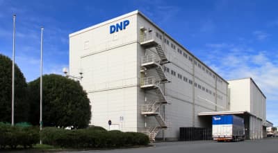
Exterior view of the Kuki Plant / TGV glass core substrate pilot line
In a parallel move, the major Japanese printing and materials supplier Dai Nippon Printing (DNP) recently announced the installation of a pilot line for TGV glass core substrates at its Kuki Plant in Saitama Prefecture. The pilot line is being established to support next-generation semiconductor packaging and is set to begin phased operation shortly, with high-quality samples scheduled to be provided in early 2026.
The pilot line will be used to verify mass production technologies for TGV glass core substrates, which DNP developed in 2023 as an alternative to conventional organic core substrates. With the rapid adoption of chiplet-based designs, traditional organic substrates are increasingly challenged by insufficient flatness, difficulties in fine-line wiring, and warpage caused by limited rigidity. Glass core substrates offer improved flatness, higher stiffness, and better suitability for fine interconnect formation.

DNP's TGV glass core substrates are designed for FC-BGA packaging and are positioned between the motherboard and semiconductor chips. The products feature numerous through-glass vias that enable electrical connections between the chip and the board. With a panel size of 510 by 515 millimeters, the substrates meet the flatness and rigidity requirements of next-generation packaging while enabling higher via density than organic resin-based materials.
The company offers both copper-filled via structures and conformal via designs, targeting high-aspect-ratio, high-quality products where its technical strengths can be fully leveraged. Looking ahead, DNP plans to refine its production system based on customer feedback and market demand, with the goal of launching mass production around fiscal year 2028. The project also supports the ongoing transformation of the Kuki Plant by optimizing human resources and facilities originally dedicated to traditional printing operations.
+86 191 9627 2716
+86 181 7379 0595
8:30 a.m. to 5:30 p.m., Monday to Friday
