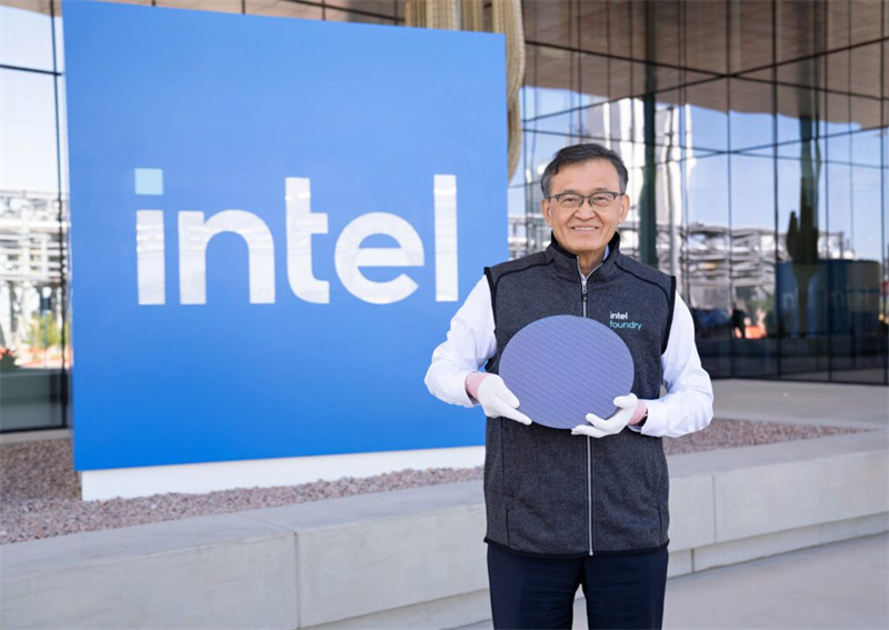
Intel is making one of the boldest bets in its history as it races to reclaim its position as a global semiconductor leader. On the desert floor of Chandler, Arizona, the company has invested more than $20 billion into Fab 52, a next-generation manufacturing facility that stands at the center of Intel's comeback strategy — and America's broader effort to rebuild its advanced chipmaking capabilities.
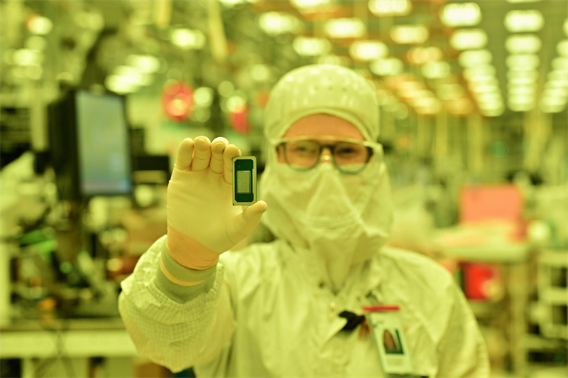
Inside the four-story facility, Intel is deploying its most advanced process node, Intel 18A, to manufacture leading-edge chips in the United States for the first time in nearly a decade. The fab is equipped with ASML's extreme ultraviolet (EUV) lithography systems, each costing around $250 million, marking a return to state-of-the-art production technology that Intel once pioneered but later struggled to keep up with.
Intel has recently hosted a series of tours for potential foundry clients at Fab 52 as it pushes to expand its Intel Foundry Services (IFS) business — positioning itself as an alternative to Taiwan Semiconductor Manufacturing Co. (TSMC) and Samsung for external chip manufacturing. Analysts, however, note that most chip designers remain cautious, waiting to see whether Intel can perfect its new process for its own products before entrusting it with theirs.
Intel's Technological Turning Point: The 18A Process
The Intel 18A process — equivalent to the industry's 2-nanometer class — represents a critical leap for the company. It introduces two key innovations:
● RibbonFET, Intel's first new transistor architecture in over a decade, allowing for tighter transistor density and faster switching speeds.
● PowerVia, a backside power delivery system that routes power beneath the transistors, improving energy efficiency and signal integrity.
Together, these technologies deliver up to 15% better performance per watt and 30% higher transistor density compared to Intel 3, the company's previous leading node. Intel says this design also reduces power interference, enabling denser and more efficient chips suitable for artificial intelligence (AI), cloud computing, and high-performance PC applications.
The 18A node was developed and qualified at Intel's Oregon research hub and is now ramping toward high-volume manufacturing at Fab 52. It will form the foundation for at least three future generations of Intel products — both for consumer PCs and data center platforms.
Panther Lake: The First AI PC Platform on Intel 18A
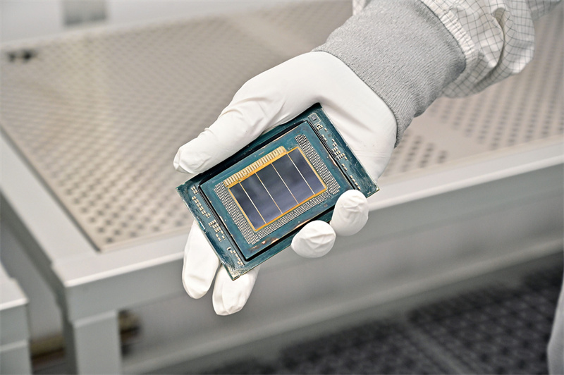
At its October 9, 2025 event, Intel unveiled the Intel Core Ultra Series 3, codenamed Panther Lake — the company's first product built on the Intel 18A process. The chip is designed to power the next generation of AI PCs, gaming devices, and edge systems, delivering a balance of high performance and power efficiency.
Panther Lake introduces a scalable multi-chiplet architecture, giving partners flexibility across form factors and price points. It features up to 16 new performance and efficiency cores, a redesigned Intel® Arc™ GPU with 12 Xe cores, and up to 180 TOPS (trillions of operations per second) of AI performance. The result is over 50% faster CPU and GPU performance compared with its predecessor, alongside significantly improved power efficiency.
Beyond PCs, Intel plans to extend Panther Lake's capabilities to robotics and industrial AI applications. A new Intel Robotics AI suite and reference board allow developers to build cost-effective AI-powered robots for control and perception tasks. High-volume production of Panther Lake is expected to ramp up by the end of this year, with broad market availability starting in January 2026.
Clearwater Forest: The First Intel 18A Xeon Processor
Intel also previewed Clearwater Forest, branded as Intel Xeon 6+, the company's most efficient server processor to date and its first data center product built on Intel 18A. Targeted at hyperscale cloud providers, data centers, and telecom networks, Clearwater Forest features up to 288 E-cores and delivers a 17% improvement in Instructions Per Cycle (IPC) over its predecessor.
By improving density, throughput, and power efficiency, the chip aims to help large-scale operators reduce costs and scale AI workloads more efficiently. Intel plans to launch Xeon 6+ in the first half of 2026.
Fab 52: A Cornerstone of Intel's U.S. Manufacturing Revival
Fab 52 is Intel's fifth high-volume manufacturing plant on its Ocotillo campus in Chandler, part of a broader $100 billion U.S. investment plan that also includes R&D operations in Oregon and packaging facilities in New Mexico. Together, these sites form a vertically integrated ecosystem for advanced chipmaking, from research to mass production and packaging.
Intel CEO Lip-Bu Tan, who took over in March, described Fab 52 as "mission critical, not just for Intel but for our country." He highlighted that the company's manufacturing resurgence supports U.S. strategic goals for semiconductor self-reliance and supply chain resilience. In August, Intel secured an $8.9 billion investment from the U.S. government under the CHIPS and Science Act, representing one of the largest public-private semiconductor investments since 2008.

Challenges and Industry Outlook
Despite strong progress, Intel still faces significant challenges. Yield rates for its 18A process reportedly lag behind TSMC's leading-edge 2nm node, and the company must prove that its new process and product lines can achieve stable, cost-effective mass production.
Analysts note that if Intel can demonstrate high yields and strong product performance at Fab 52, it could attract major customers such as NVIDIA, AMD, or Apple to its foundry services — filling the fab's remaining capacity and driving a new phase of U.S.-based semiconductor growth.
"Fab 52 is like a shopping center that needs an anchor tenant," said Patrick Moorhead of Moor Insights & Strategy. "If Intel can prove 18A's reliability and land one big customer, it will be game on."
A Defining Moment for U.S. Chipmaking
The success of Fab 52 and the Intel 18A process will determine whether Intel can fully reestablish itself as both a top-tier chip designer and a global foundry player. More broadly, it will test whether America can reclaim its leadership in the most advanced segments of semiconductor manufacturing — an industry critical to everything from AI to national security.
As Intel's CTO Sachin Katti summarized, "We're making two big bets — on our technology and our capacity. The outcome will define not only Intel's future, but the future of U.S. semiconductor leadership."
+86 191 9627 2716
+86 181 7379 0595
8:30 a.m. to 5:30 p.m., Monday to Friday

