On July 30, Japan-based Inspec announced the launch of two next-generation systems targeting advanced semiconductor package substrates: the SX7000 series inspection system and the LX7000 laser repair system. Both are designed to meet the growing demand for high-density, chiplet-based substrates used in AI servers and data centers.
Driven by the explosive growth of generative AI, global investment in AI data centers is surging. This has accelerated adoption of chiplet architecture—where multiple smaller dies with different functions are interconnected within a single package—and increased demand for high-density interposers. These trends are placing new demands on substrate miniaturization and inspection precision.
The SX7000 series (models SX7300 and SX7400) supports line/space (L/S) resolutions of 2.0μm/2.0μm and 1.5μm/1.5μm, addressing the inspection needs of next-gen high-resolution substrates. It accommodates panel sizes up to 615mm × 515mm and is built with dimensions of 1,590mm (W) × 2,450mm (D) × 2,255mm (H), weighing approximately 2,800kg.
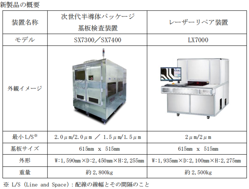
The newly launched LX7000 laser repair system also supports 2μm/2μm L/S and the same substrate size. It measures 1,935mm (W) × 2,100mm (D) × 2,275mm (H) and weighs approximately 2,500kg. Both systems support advanced pattern recognition and ultra-fine defect correction, providing an integrated solution from inspection to repair.
Together, these tools offer manufacturers a comprehensive path to improve production efficiency and yield while addressing the growing complexity of chiplet-based packaging.

Outlook
Inspec estimates about one year from order to delivery and acceptance for the new equipment. As a result, the new systems are not included in the company's earnings forecast for the April 2026 fiscal year. The company will monitor demand and disclose updates as necessary.
By combining advanced inspection and repair capabilities, Inspec aims to support the evolving requirements of AI-era semiconductor packaging.
+86 191 9627 2716
+86 181 7379 0595
8:30 a.m. to 5:30 p.m., Monday to Friday

