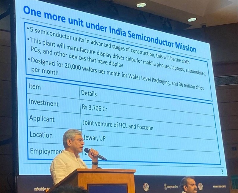
On May 14, India's Union Cabinet approved a ₹3,706 crore (approximately $435 million) investment plan by a joint venture between Taiwan's Foxconn and India's HCL Group to establish a semiconductor packaging facility near Jewar Airport in Uttar Pradesh. The plant will have a monthly wafer-level packaging capacity of 20,000 wafers and is expected to produce up to 36 million display driver chips annually for mobile phones, laptops, and automobiles. Commercial production is slated to begin in 2027.
The facility, India's sixth approved under its national semiconductor mission, will span 48 acres in Sector 28 of the YEIDA industrial area and create approximately 2,000 jobs. The land has been allocated to Vama Sundari Investments (Delhi) Private Limited (VSIPL), a major HCL Group promoter. Foxconn will hold a 40% stake in the venture through its subsidiary Foxconn Hon Hai Technology India Mega Development.
To support the project, the Uttar Pradesh government has offered substantial incentives, including capital subsidies, land rebates, tax waivers, and support for infrastructure and workforce development. Once operational, the plant is expected to meet 40% of India's domestic demand for display driver chips and support Foxconn's global supply needs.
This announcement comes amid mixed progress in India's semiconductor ambitions. While some major projects, such as the $10 billion Adani-Tower Semiconductor fab and Zoho's planned compound semiconductor facility, have been paused or abandoned, other initiatives continue to advance. These include Tata's $11 billion fab in partnership with Taiwan's Powerchip, a $2.7 billion OSAT facility by Micron, and Renesas Electronics' $912 million collaboration with CG Power and Stars Microelectronics.
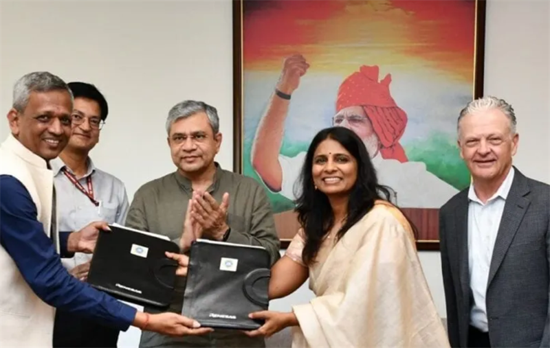
On the same day, Japan's Renesas Electronics announced expanded partnerships with India's Ministry of Electronics and IT (MeitY) to strengthen the local semiconductor ecosystem. Renesas signed two MoUs with MeitY's Centre for Development of Advanced Computing (C-DAC) under the Design-Linked Incentive (DLI) and C2S (Chips-to-Startup) programs. These agreements aim to support startups and academic institutions in VLSI and embedded semiconductor systems, enhancing indigenous innovation and product engineering.
Renesas also opened new state-of-the-art offices in Bengaluru and Noida to accommodate its growing R&D teams. The Bengaluru site, now the company's largest in India, houses 500 staff and features cutting-edge design labs and support facilities. The Noida office brings engineering and business units together to accelerate development in high-performance automotive computing.
India remains a key growth market for Renesas, with ambitions for the country to contribute over 10% of its global revenue by 2030. The company plans to grow its India workforce to 1,000 employees by the end of 2025 and continues to deepen collaborations with local startups, academia, and industry partners in support of India's goal of semiconductor self-reliance.
+86 191 9627 2716
+86 181 7379 0595
8:30 a.m. to 5:30 p.m., Monday to Friday

