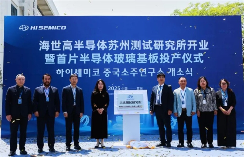
On April 25, Hi SEMICO Semiconductor Technology (Suzhou) Co., Ltd. (provisional translation based on public information; official English name not yet confirmed) officially launched production of its first semiconductor-grade glass substrate and inaugurated its new Testing Research Institute in Suzhou High-Tech Zone.
The facility marks a significant breakthrough in China's push for domestic alternatives to high-end semiconductor equipment, particularly in the field of Through-Glass Via (TGV) metal deposition. Long reliant on imported systems, China's semiconductor industry has faced persistent bottlenecks due to foreign dominance in core process technologies. Hi SEMICO Suzhou's new full-size TGV glass substrate metallization line—the first of its kind in China open for commercial services—features a "dry-in, dry-out" process flow that enhances production efficiency and transparency while advancing localization.
Hi SEMICO Suzhou's CEO, Cao Longji, emphasized the company's mission to accelerate the localization of TGV technologies through parallel technology transfer, independent R&D, and continuous product innovation. The new institute will focus on process development, testing, and data analysis for advanced packaging technologies, driving forward the domestic substitution of key semiconductor manufacturing equipment.
At the launch event, Hi SEMICO Suzhou signed strategic cooperation agreements with several leading industry players, including the Jiangsu Display Industry Alliance, DJ-Semicon, and Suzhou Axtek Photoelectric Technology Co.,Ltd. The company also honored outstanding suppliers that have supported core component delivery and process chain collaboration, highlighting a shared commitment to innovation and mutual growth within the supply chain.
Representatives from the National Flat Panel Display Metrology Center and the Jiangsu Display Industry Alliance jointly unveiled the plaque for the new Testing Research Institute, which will serve as a hub for advancing technologies such as TGV and TSV (Through-Silicon Via).

Founded through a joint investment by South Korea's Hi SEMICO and a Chinese team, Hi SEMICO Suzhou was introduced to Suzhou in 2024 through the High-Tech Zone's Technology Investment Center. Hi SEMICO, established by Han Min-seok—winner of the prestigious Jang Young-sil Award—pioneered the vertical metal deposition system and is a leading supplier to global materials companies such as SKC. Its customer base includes major names like Samsung, LG, and SK Hynix.
Guests at the event also toured Hi SEMICO Suzhou's glass substrate production facility, where the company showcased its advanced manufacturing capabilities. Looking ahead, Hi SEMICO Suzhou plans to deepen collaboration with universities and research institutes and aims to achieve 100% localization of its production line equipment within two years.
About Hi SEMICO
Hi SEMICO specializes in providing equipment solutions for the semiconductor and high-end PCB (Printed Circuit Board) industries.Its products are supplied across various fields, including TGV/TSV/WLP/PLP electroplating, driver ICs, COF, PKG PCBs, and 5G PCB surface treatment. The company continuously invests in R&D and has built experienced in-house teams for design, manufacturing, and other core capabilities.
Hi SEMICO independently develops precision equipment essential for semiconductor packaging, enabling it to quickly respond to the rapidly evolving needs of semiconductor and PKG PCB production lines. By offering customized equipment solutions tailored to customer requirements, Hi SEMICO ensures outstanding product quality and comprehensive, responsive service to support its clients' success.
+86 191 9627 2716
+86 181 7379 0595
8:30 a.m. to 5:30 p.m., Monday to Friday

