South Korea's FNS Tech announced on September 25 that it has developed chemical mechanical polishing (CMP) pads for semiconductor glass substrates.
CMP pads are used to planarize substrates. In the case of glass substrates, after through-glass vias (TGV) are formed via wet etching, copper is filled in to enable signal transmission. FNS Tech's newly developed pads can flatten copper layers on glass substrates during this process.
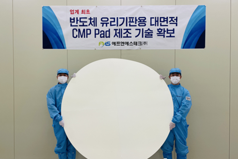
To accommodate large-area glass panels, the company designed oversized pads leveraging expertise built in OLED and other display processes. FNS Tech confirmed it has secured the necessary technology and successfully produced prototypes.

The company has filed four patents, including one for large-area polishing pads with a scalable structure. "With this industry-first glass substrate CMP pad, we aim to gain an early foothold in a new market," an FNS Tech official said.
Glass substrates are emerging as a key next-generation technology. As demand for high-performance semiconductors accelerates with artificial intelligence (AI), glass is gaining attention as a promising alternative substrate material. This trend is driving the development of related materials, components, and equipment technologies toward commercialization.
+86 191 9627 2716
+86 181 7379 0595
8:30 a.m. to 5:30 p.m., Monday to Friday

