The U.S. Department of Defense and the state of Texas are investing USD 1.4 billion to build a new advanced packaging facility in Austin dedicated to next-generation 3D heterogeneous integration (3DHI). Announced recently under DARPA's Next-Generation Microelectronics Manufacturing (NGMM) program, the project aims to close the long-standing gap between laboratory prototypes and manufacturable hardware for defense and commercial applications.
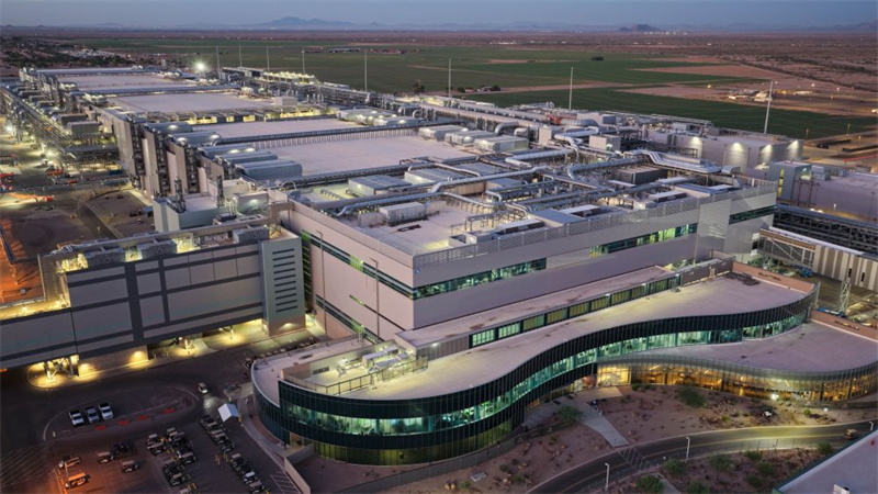
The facility, operated by the University of Texas at Austin's Texas Institute for Electronics (TIE), is being built inside a refurbished 1980s-era semiconductor plant. It will focus on stacking and integrating diverse chip types and materials—including silicon, gallium nitride, and photonics—to overcome the limits of traditional monolithic fabrication. Texas will contribute USD 552 million, with DARPA providing the remaining USD 840 million.
Unlike conventional fabs designed for high-volume output, the Austin site will support high-mix, low-volume production, allowing startups, researchers, and defense contractors to prototype unconventional devices that mainstream foundries cannot easily accommodate.
DARPA program manager Michael Holmes described 3DHI as a potential "revolution in microelectronics," noting that silicon-on-silicon stacking can deliver roughly 30× performance gains, while integrating dissimilar materials could achieve up to 100× improvements.
Key technical work includes developing a new process design kit (PDK) and assembly design kit (ADK) to standardize how multiple materials can be combined vertically—a foundational requirement for reproducible 3DHI manufacturing. NGMM will validate these capabilities through three demonstration systems: a phased-array radar, an infrared focal-plane array, and a compact power converter.
The fab will also deploy AI-assisted process modeling from local startup Sandbox Semiconductor to improve yields across diverse prototype workflows.

The initiative arrives as the global semiconductor industry shifts toward multi-chip and 3D packaging. Intel, AMD, Nvidia, Apple, and TSMC all rely on advanced integration to keep performance scaling alive. But DARPA's project differs in scope: instead of optimizing silicon chiplets, NGMM is focused on blending entirely different device classes—sensors, power amplifiers, logic, and photonics—into a single advanced package.
The program complements broader U.S. industrial-policy efforts, including the CHIPS and Science Act's National Advanced Packaging Manufacturing Program and new domestic facilities from Intel and Amkor. Together, these initiatives aim to rebuild an end-to-end advanced packaging ecosystem on U.S. soil.
TIE CEO Dwayne LaBrake called the project "a startup with more runway than most," noting the goal is to transition into a self-sustaining commercial operation within five years, supported by national-security customers and specialty manufacturing needs.
If successful, the Austin facility could become a critical hub for next-generation defense electronics and a cornerstone of America's emerging advanced packaging strategy.
+86 191 9627 2716
+86 181 7379 0595
8:30 a.m. to 5:30 p.m., Monday to Friday

