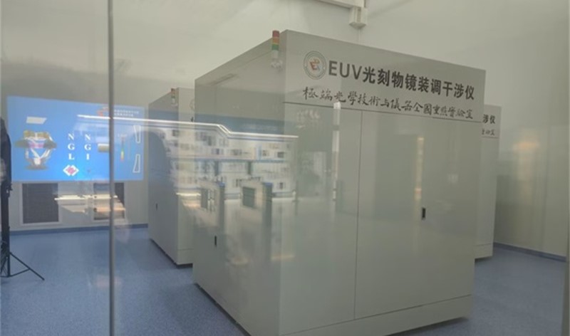
A major shift may be underway in the global lithography landscape, as China edges closer to introducing its first domestically developed extreme ultraviolet (EUV) lithography machine. According to recent media reports, a Chinese research team has achieved a key breakthrough by developing an EUV system based on laser-induced discharge plasma (LDP)—a radically different approach from that of industry giant ASML.
Unlike ASML's laser-produced plasma (LPP) technology—which requires high-energy lasers to strike tin droplets and a complex FPGA-based control system—China's LDP method involves vaporizing tin between electrodes and applying high-voltage discharge to create plasma. The resulting 13.5nm EUV radiation, produced through electron-ion collisions, is essential for advanced chip manufacturing at 7nm nodes and below.
Early test data indicates that the LDP-based prototype offers several key advantages: a simpler architecture, smaller physical footprint, lower energy consumption, and significantly reduced manufacturing costs. These characteristics suggest a potential breakthrough not just in technology, but in challenging the cost and complexity of traditional EUV systems.
Trial production of the new machine is reportedly targeted for the third quarter of 2025, with its debut seen as a milestone in China's efforts to close its EUV gap and gain independence from Western-controlled supply chains. The system—believed to be named Hyperion-1—features components such as a 50W Yb fiber laser, Mo/Si multilayer mirrors (65% reflectivity), and a RISC-V-based plasma control system, alongside innovations like carbon nanotube-cooled optics. Though its current output is limited to around 10 wafers per hour, a follow-up model—Hyperion-2, expected by 2026—aims to reach 150W power and support commercial-scale production.
Trial images shared by X accounts @zephyr_z9 and @Ma_WuKong suggest that testing is underway at Huawei's Dongguan facility. A separate report attributes the development of the LDP-based EUV light source to a research team from Harbin Provincial Innovation, whose system reportedly meets the 13.5nm wavelength requirement critical for modern photolithography. Together, these efforts reflect growing momentum behind China's EUV ambitions.
China's foundries, particularly SMIC, have long faced challenges producing chips below 7nm due to a lack of access to EUV tools. Existing DUV-based multi-patterning techniques have proven costly, inefficient, and low-yield—reportedly making 5nm chips up to 50% more expensive than those produced by leading global foundries. The lack of access to ASML's state-of-the-art EUV systems—due to export controls imposed by the U.S. and its allies—has further limited China's ability to compete at the highest levels of semiconductor manufacturing.

The LDP-based EUV machine, if successfully scaled, could reverse this dynamic. It holds strategic implications not only for China's semiconductor roadmap but also for its broader ambitions in AI, advanced computing, and digital sovereignty. Potential applications include powering domestic chip lines such as Ascend 930, 920B, and 910D, used in AI and high-performance computing.
While the current generation still lags behind ASML's systems in throughput and maturity, the shift to an alternative architecture represents a bold technological divergence—one that seeks to bypass patents, reduce foreign reliance, and gradually chip away at entrenched monopolies in the semiconductor value chain.
China's EUV efforts are still in their early stages, and challenges such as throughput, durability, and ecosystem integration remain. But with sustained investment and a narrowing focus on core bottlenecks, China may be on the cusp of a significant leap in lithography—one that could redefine the next chapter of the global chip race.
+86 191 9627 2716
+86 181 7379 0595
8:30 a.m. to 5:30 p.m., Monday to Friday

