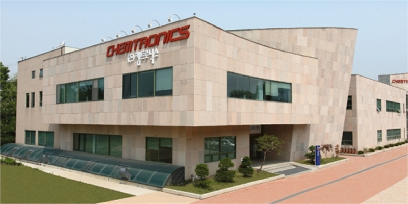
South Korean company Chemtronics (KOSDAQ: 089010) announced on August 26 that it has begun building a pilot production line for Through Glass Via (TGV) technology, a key process in manufacturing semiconductor glass substrates. The move marks a significant step in the company's effort to commercialize glass-based packaging, which is increasingly seen as a next-generation alternative to organic substrates.
Glass substrates are thinner and flatter than traditional plastic-based PCBs, enabling finer circuit patterns and offering advantages such as higher density, improved flatness, stable coefficient of thermal expansion (CTE), and low dielectric properties. These features make them well suited for advanced semiconductor packaging in applications like AI processors, high-bandwidth memory (HBM), fan-out, and 2.5D/3D integration.
Chemtronics has placed an order for laser processing equipment from Germany's LPKF, along with automated optical inspection (AOI) and X-ray systems, to be installed at J3's Cheonan plant, which it acquired earlier this year. The pilot line is scheduled for completion by the end of October, with sample products to be delivered to customers by year-end.

The TGV process involves drilling tens to hundreds of micron-scale holes into glass substrates to create electrical interconnections. Chemtronics plans to combine laser drilling with wet etching to enhance hole quality and product strength. The company has also secured a supply chain for specialized glass materials resistant to hydrofluoric acid, differentiating its approach from conventional alkali-based etching methods.
Beyond equipment orders, Chemtronics is leveraging J3's chemical mechanical polishing (CMP) and cleaning capabilities to ensure flatness and particle control in the post-processing stage. Together, the company will cover nearly the full TGV process flow in-house, with only plating outsourced.
Building on its prior experience in display glass processing and hybrid OLED etching, Chemtronics expects to expand into mass production of semiconductor glass substrates as early as late 2026 or 2027. The company also plans to construct a dedicated semiconductor glass substrate and materials line on a 6,600-square-meter site at the Cheonan facility, while developing etching and wastewater treatment infrastructure in Sejong and Cheonan.
A company representative said, "We aim to supply prototype products to customers by the end of this year and begin full-scale discussions on mass production. As demand for high-performance semiconductors grows, we believe glass substrates will become a critical platform for the next generation of packaging."
+86 191 9627 2716
+86 181 7379 0595
8:30 a.m. to 5:30 p.m., Monday to Friday
