Canon, the Japanese company known for its printers and cameras, unveiled an innovative solution on Friday, Oct. 13, which is designed to aid in the production of cutting-edge semiconductor components.

Canon’s recently introduced “nanoimprint lithography” system represents the company’s competitive response to Dutch firm ASML, a dominant force in the extreme ultraviolet (EUV) lithography machine sector. ASML’s machinery is essential for producing cutting-edge chips, including those used in the latest Apple iPhones.
The utilization of these machines has been drawn into the technological conflict between the United States and China. The United States, employing export restrictions and diverse sanctions, has aimed to obstruct China's access to crucial chips and manufacturing machinery, hampering the progress of the world's second-largest economy in a field where it is already perceived as lagging.
ASML's EUV technology has gained significant traction among leading chip manufacturers due to its crucial role in enabling the production of semiconductors at 5 nanometers and below. This nanometer measurement pertains to the size of chip features, with smaller values accommodating more features on a chip, consequently enhancing semiconductor performance.

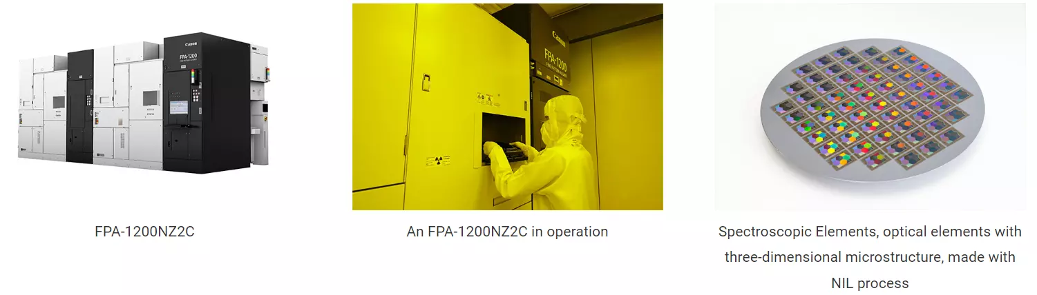
Canon reportedly announced that its new system, the FPA-1200NZ2C, can produce semiconductors matching a 5nm process and scale down to 2nm, surpassing the capabilities of the A17 Pro chip found in Apple's iPhone 15 Pro and Pro Max, which is a 3nm semiconductor.
 Features
In contrast to conventional photolithography equipment, which transfers a circuit pattern by projecting it onto the resist coated wafer, the new product does it by pressing a mask imprinted with the circuit pattern on the resist on the wafer like a stamp. Because its circuit pattern transfer process does not go through an optical mechanism, fine circuit patterns on the mask can be faithfully reproduced on the wafer. Thus, complex two- or three-dimensional circuit patterns can be formed in a single imprint (a pattern forming process of nanoimprinting), which may reduce the cost of ownership (CoO).
Canon's NIL technology enables patterning with a minimum linewidth of 14 nm (one billionth of a meter), equivalent to the 5-nm-node (nm-node”: a generation of semiconductor technology) required to produce most advanced logic semiconductors which are currently available. Furthermore, with further improvement of mask technology, NIL is expected to enable circuit patterning with a minimum linewidth of 10 nm, which corresponds to 2-nm-node.
The new product employs newly developed environment control technology that suppresses the contamination with fine particles in the equipment. This enables high-precision alignment which is necessary for the manufacture of semiconductors with an increasing number of layers and the reduction of defects due to fine particles, and enables the formation of fine and complex circuits, contributing to the manufacture of cutting-edge semiconductor devices.
Since the new product does not require a light source with a special wavelength for fine circuit, it can reduce power consumption significantly compared to the photolithography equipment for currently available most advanced logic semiconductors (5-nm-node with 15 nm linewidth), thereby contributing to CO2 reduction.
The new product can be used for a wide range of applications, such as metalenses (an element with the same function as a lens by controlling light with a fine structure smaller than the wavelength of visible light) for XRs with microstructures of tens of nanometers, in addition to logic and other semiconductor devices.
The Dutch government has imposed restrictions on ASML, preventing the export of its EUV lithography machines to China, where no units have been shipped. This limitation exists due to the critical role of these machines in the production of cutting-edge semiconductor chips.
With Canon's assertion that their new machine can facilitate the production of semiconductors equivalent to 2nm, it is likely to face increased scrutiny.
▼▼▼
Samsung Pulls Out ‘236-Layer’ Card for Xi’an NAND Factory following US Regulatory Reprieve
Chipmaker Qualcomm to lay off more than 1,200 staff in California
Israel-Hamas Conflict Threatens an Already-Vulnerable Chip Industry
Toshiba Acquired by JIP for $14 Billion, Set to Delist in Japan
Tsinghua University Unveils World's First Fully Integrated Memristor Chip
BH Co., Ltd. Announces Major Investment in New Vietnam Facility
......
Read more latest news about the PCB and semiconductor industry here
+86 191 9627 2716
+86 181 7379 0595
8:30 a.m. to 5:30 p.m., Monday to Friday

