ASML and Nikon made major announcements this week, unveiling new lithography systems that underscore growing competition in the global semiconductor equipment market. Lithography, which defines critical dimensions in chips, accounts for roughly 35% of overall semiconductor manufacturing costs and is a key factor in determining production precision and efficiency.
ASML Accelerates High-NA EUV Deployment
On July 16, Dutch company ASML, the world's only supplier of extreme ultraviolet (EUV) lithography systems, reported second-quarter 2025 financial results. The company posted €7.7 billion in net sales and €2.3 billion in net profit, with €2.3 billion worth of EUV orders contributing to a total of €5.5 billion in new bookings. During the quarter, ASML shipped 67 lithography systems, including 11 EUV units.
ASML also confirmed it delivered the first TWINSCAN EXE:5200B, its second-generation High-NA EUV lithography system, with Intel as the reported buyer. The EXE:5200B can process more than 220 wafers per hour—up from 185 wafers on the previous EXE:5000—and features a numerical aperture (NA) of 0.55, significantly improving precision over the 0.33 NA in earlier EUV tools.
The company emphasized that AI remains a key driver of demand, with chipmakers such as NVIDIA, Intel, and TSMC scaling up AI data center construction, requiring more advanced lithography equipment. High-NA EUV is considered essential for 2nm and future Angstrom-class nodes and is expected to shape semiconductor manufacturing for the next decade.
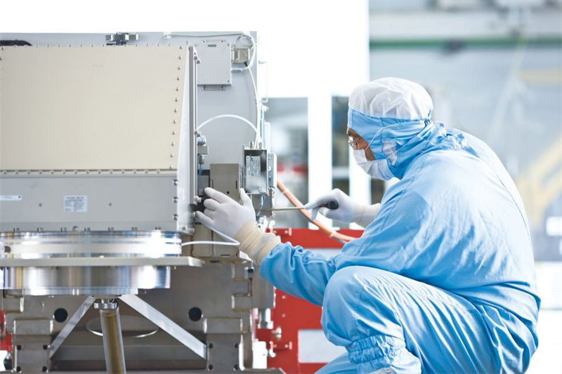
Nikon and Canon Target Advanced Packaging
Meanwhile, Japan's Nikon and Canon are taking a differentiated approach by focusing on advanced packaging and mature node markets. On the same day, Nikon announced that its new DSP-100 lithography system, designed for backend semiconductor packaging, is now open for orders, with a planned launch in fiscal 2026.
The DSP-100 uses maskless SLM (spatial light modulator) technology, eliminating the need for traditional photomasks and cutting development costs by over 40%. It supports 1μm line/space resolution with overlay accuracy within ±0.3μm and handles panels up to 600mm square. The system targets fan-out panel-level packaging (FOPLP), a growing segment for AI and high-performance computing (HPC) chips. Nikon expects to capture 20% of the FOPLP market post-launch and has reportedly received preliminary orders from major OSATs.

Canon, which primarily produces i-line lithography tools, shipped 233 semiconductor lithography units in 2024, generating $1.65 billion in revenue. In October 2023, Canon launched the world's first commercial nanoimprint lithography (NIL) system, the FPA-1200NZ2C. In September 2024, the company delivered its first NIL tool to Texas' Advanced Research Institute for semiconductor R&D.
Unlike EUV, Canon's NIL technology creates nanoscale patterns by physical imprinting, enabling sub-5nm resolution without requiring complex optics. Canon claims throughput of 130 wafers per hour, with plans to increase this to 180 wafers by 2026—approaching EUV levels.
Outlook
While ASML continues to dominate the high-end lithography segment, Nikon and Canon are carving out opportunities in advanced packaging and alternative lithography technologies. With new architectures like chiplets and growing AI demand reshaping chip design, the competition in the lithography market is poised to intensify.
+86 191 9627 2716
+86 181 7379 0595
8:30 a.m. to 5:30 p.m., Monday to Friday

