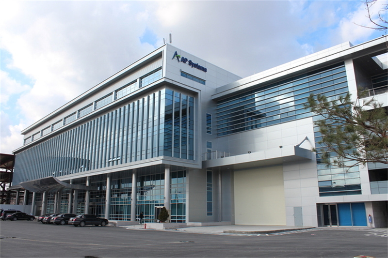
AP System has officially launched research and development efforts for glass substrate manufacturing equipment, a move that could position the company for long-term growth in advanced semiconductor packaging. The initiative involves internal foundational research following the transfer of glass-through-via (TGV) technology and related personnel from its holding company, APS Holdings. While the project is still in its early stages, with no specific processes or product specifications yet determined, the company aims to secure core technologies ahead of expected commercialization around 2027–2028.
The glass substrate business, initially driven by APS since last year, has now been transferred to AP System for further development. APS previously identified glass substrates as a mid-to-long-term strategic focus and has hinted at expanding beyond equipment to substrate sales in the future.
Unlike traditional organic or silicon-based substrates, glass substrates offer several advantages: lower thermal expansion, minimal warping under high heat, and up to 10 times greater signal transmission within the same area. These properties make them highly attractive for next-generation, high-performance semiconductors, particularly as demand for AI chips accelerates.
According to research firm MarketsandMarkets, the global glass substrate market is expected to grow from $7.1 billion in 2023 to $8.4 billion by 2028, fueled by increasing semiconductor complexity and miniaturization. This growth is intensifying global competition around glass substrate technologies.

Industry observers have noted potential synergy between AP System and Samsung, especially as Samsung Electro-Mechanics (SEMCO) begins pilot production of glass substrates at its Sejong facility in Q2 2025, targeting mass production by 2027. This raises the possibility that AP System could emerge as a future equipment supplier. APS Holdings previously confirmed ongoing discussions between AP System and SEMCO regarding glass substrate equipment collaboration.
While the company has declined to confirm any specific client partnerships, a spokesperson said, “The development of glass substrate equipment is still at an early stage. We're currently conducting internal R&D, and detailed specs or timelines haven't been set.”
As part of its strategic pivot, AP System has also added two semiconductor veterans from Samsung to its board of directors. Former SEMCO executive vice president Yoo Ho-sun has been appointed both CEO and board chair, while former SEMCO executive Hwang Shin-hwan has joined as an outside director. Both Yoo and Hwang, alumni of Seoul National University's control and instrumentation engineering program, bring deep expertise in semiconductor production and equipment development.
AP System is positioning this leadership shift as part of a broader push to diversify beyond its display-centric portfolio. In 2023, displays accounted for over 88% of the company's ₩516.7 billion in consolidated revenue, while the semiconductor division contributed just 10%. The company aims to expand semiconductor-related sales, particularly in areas like high-bandwidth memory (HBM) and advanced packaging technologies based on glass substrates and interposers.
A company representative noted, “The OLED smartphone market has been relatively stagnant, impacting our core display equipment business. We're focusing on high-growth areas like semiconductors, where we can leverage our expertise in laser equipment across more process steps.”
Analysts also see the structural shift as promising. A recent report by Shinhan Investment's Nam Goong-hyun stated, “While last year's semiconductor revenue growth was slower than expected, the direction of portfolio expansion remains valid. Continued growth in RTP and laser equipment shipments is expected this year.”
+86 191 9627 2716
+86 181 7379 0595
8:30 a.m. to 5:30 p.m., Monday to Friday
