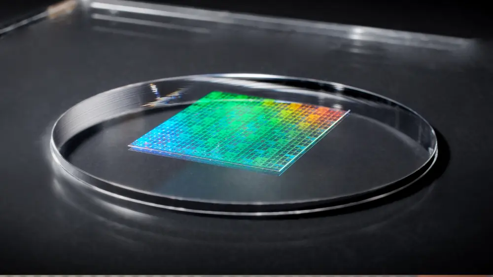
According to information obtained in December 2025, innovative Japanese semiconductor supplier Dai Nippon Printing (DNP) has successfully developed a nanoimprint lithography (NIL) template capable of achieving 10nm line widths, suitable for logic circuit patterning equivalent to a 1.4nm process node. The company has initiated customer evaluations and plans to begin mass production in 2027, aiming to increase NIL-related revenue to 4 billion yen (approximately 1.8 million RMB) by fiscal year 2030.
DNP positions the new NIL technology as a complementary solution to extreme ultraviolet (EUV) lithography, which continues to advance in response to growing demand for advanced logic semiconductors in smartphones, data centers, and other high-performance applications. While EUV has become the industry standard, its high investment cost, energy consumption, and environmental impact have led manufacturers to explore alternatives. NIL, first researched by DNP in 2003, stamps pre-formed circuit patterns directly onto wafers, offering the potential to reduce exposure energy by up to 90% compared with conventional EUV processes.
The new 10nm line-width NIL template integrates DNP’s long-standing expertise in high-precision photomask fabrication with advanced wafer process technology. The approach incorporates self-aligned double patterning (SADP) techniques and precise thin-film deposition and etching, enabling the doubling of pattern density while maintaining dimensional accuracy and stability required for advanced logic circuits. By replacing select EUV steps, the process can lower overall fab energy consumption to roughly one-tenth of current mainstream methods, providing manufacturers with more flexible and cost-efficient patterning options.
Canon, which has also pursued NIL as a lower-power alternative to EUV, has begun shipping its first 300mm NIL tools to early research partners. Together, these developments highlight the potential for nanoimprint lithography to reduce lithography power consumption by up to 90% for advanced nodes, even as companies like TSMC and Samsung prepare for 1.4nm mass production. NIL is not intended to fully replace EUV but could complement it for specific layers, potentially cutting costs and energy usage on high-volume logic production lines.

DNP has actively engaged with semiconductor manufacturers to conduct technical evaluations of the new NIL technology and plans to establish a mass-production supply chain ahead of the 2027 launch. The company will also showcase the 10nm NIL template at SEMICON Japan 2025, held at Tokyo International Exhibition Center from December 17 to 19, to promote industry collaboration and accelerate adoption.
Looking forward, DNP intends to continue advancing NIL technology and expanding production capacity to position the business as a key growth driver within its semiconductor segment. If successful, the technology could offer manufacturers an economically and environmentally advantageous pathway to advanced logic production while supporting the ongoing miniaturization of chips for AI, cloud computing, and mobile applications.
+86 191 9627 2716
+86 181 7379 0595
8:30 a.m. to 5:30 p.m., Monday to Friday

