-advertisement-
Currently, the world's top-ranked semiconductor substrate manufacturer Ibiden (4062.T) is exploring glass substrate technology for semiconductor packaging. This indicates Ibiden's strong interest in glass substrates for semiconductor packaging. Although no company has started mass-producing glass substrates yet, industry attention towards glass substrates is increasing, particularly under the leadership of Intel.
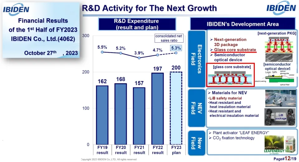
As early as late October 2023, Ibiden incorporated glass substrates into its next-generation research and development activities. The image of the glass core substrate introduced by Ibiden last October is similar to the method of another Japanese semiconductor substrate company, Shinko.
The Young's Modulus of glass substrates is four times that of traditional organic materials, reaching 70-80, giving it characteristics that are not easily bent. The smooth surface of glass substrates is conducive to forming fine circuits, with low signal loss. Glass substrates are expected to be mainly used for loading high-performance semiconductor products such as server CPUs and AI accelerators.
An industry insider stated: "The size of future high-end server boards will expand to 100x100mm, while traditional resin substrates have already reached the limit of 70x70mm. To accommodate the 100x100mm server board size, glass substrates may be necessary." It is expected that glass substrates will use 600x600mm glass disks with a thickness of around 0.5mm. Although the core material in glass substrates changes from resin to glass, the series of processes involving filling ABF and insulation layers are likely to be similar to existing methods.
The fact that Ibiden is in the exploration stage of glass substrate technology indicates the increasing interest of the semiconductor substrate industry in glass substrates, leading to comprehensive competition in the semiconductor packaging market:
1 Absolics and DNP: Companies that have shown early interest in glass substrates include SKC subsidiary Absolics and DNP.
Absolics, located in Covington, Georgia, is nearing completion of its factory, with the start of mass production expected to be determined by customer certification. Absolics has been producing glass substrate samples on a trial line in South Korea. DNP has set a target date of 2027 for glass substrate mass production.
2 SEMCO: President Dong-Hoon Chang stated at this year's CES that "Our goal is to establish a glass substrate production line this year, produce samples by 2025, and begin mass production after 2026."
3 LG Innotek: An official from the company stated in February this year, "I believe glass will become the main material for future semiconductor packaging substrates, and we are also considering developing glass substrates."
4 Unimicron: Taiwan-listed company Unimicron (3037.TW) has obtained glass substrate technology from the Packaging Research Center at the Georgia Institute of Technology.
5 AT&S: The Austrian company AT&S recently purchased sputtering equipment for surface plating and hole plating of glass substrates.
The glass substrate technology used by Absolics, DNP, and Unimicron originates from the Packaging Research Center at the Georgia Institute of Technology. Since 2009, GT PRC has been developing glass substrates.
Japanese company Mitsui is selling a glass carrier called High-Resolution Decoupling Panel (HRDP), which can be used for designing circuits with line widths & spacings less than 2 & 2μm. This glass carrier can be used for glass substrate research by companies facing difficulties in purchasing sputtering equipment.
Currently, some believe that in the manufacturing of fine circuits less than 2μm, glass substrates may have advantages over resin substrates, while others argue that resin substrates can also be improved to a certain extent. However, if the requirements for semiconductor substrate microcircuits drop to the 1μm level due to chip process miniaturization, the demand for glass substrates may increase.
Despite semiconductor substrate companies showing interest in glass substrates, they still face many challenges. Glass substrates, while thin and advantageous for forming fine circuits, are difficult to control, leading to low production yields and high costs.
Industry insiders point out that glass substrates must withstand the pressure applied during the filling of ABF and insulation layers, leading to issues regarding production efficiency and costs. Semiconductor substrate companies are primarily conducting research and development in glass substrates led by Intel, while also observing each other. Intel announced in September last year its plans to start mass-producing glass substrate-based semiconductors by 2030, investing $1 billion in developing glass substrate packaging technology in Arizona, USA.
Editor:King&Lulu
▼▼▼
SK Hynix plans $14.6 billion chip expansion to meet AI demand
IBM plots $730 million expansion of Canadian semiconductor site
Taiwan semiconductor firm KYEC to exit mainland China amid geopolitical tensions
Italy plans to invest €10 billion in the semiconductor industry to expand chip production
Intel Russia reports zero revenue in 2023 — now only one employee remains
Chinese researchers develop 504-qubit superconducting QC chip, build partnership for cloud access
+86 191 9627 2716
+86 181 7379 0595
8:30 a.m. to 5:30 p.m., Monday to Friday