Today's most advanced microprocessors have components just a few nanometers across, and precious few companies can produce these chips. Taiwan's TSMC owns the lion's share of the market, but Samsung is running in a distant second. The runner-up's next big chip evolution might help it gain some ground, though. Early details of Samsung's upcoming 1.4nm process node suggest future Samsung chips will offer a significant boost to power and efficiency.
Jeong Gi-Tae, vice president of Samsung Foundry, has offered up a general roadmap that could bring the company to parity with TSMC. Currently, Samsung's foundry offers 5nm (also known as SF5) manufacturing for a variety of chips. It can also manufacture 4nm and 3nm chips, but it appears Samsung only offers this technology for low-power embedded systems. Next year, Samsung will spin up a proper SF3 platform, offering customers 3nm chips with various options. However, we might not see many 3nm Samsung chips right away. Google's rumored 2024 Tensor G4 is rumored to be based on Samsung's 4nm (SF4) tech.
When 2025 rolls around, Samsung plans to update its 3nm process to SF3P, a performance, tuned version of the 3nm node. That's also when 2nm (SF2) chips will begin coming out of Samsung's foundry. This generation of Samsung chips will leverage improved gate-all-around (GAA) transistors and backside power delivery, which is reportedly the key to increasing transistor density. TSMC and Intel also plan to move to GAA for their 2nm processes.
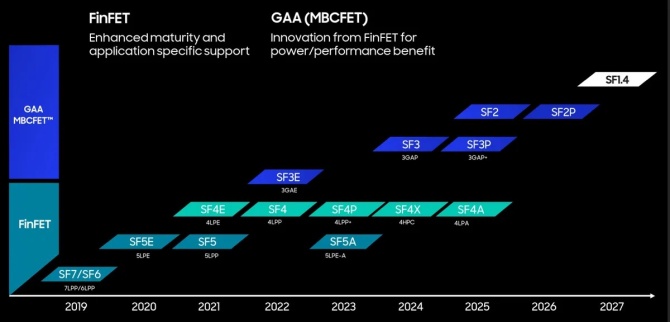
Samsung's GAA tech will come into its own in 2027 to unlock the 1.4nm process node (SF1.4). These chips will shrink components by increasing the number of GAA microsheets from three to four. With more nanosheets per transistor, these chips will offer superior current control and speed. The design will also be more able to block current leakage, which increases efficiency. At 1.4nm, we're reaching the theoretical limit of silicon-based processors. At this scale, each transistor would be just three silicon atoms wide.
Today's Samsung chips tend to underperform similar TSMC chips due to Samsung's packaging technology. As it moves toward finer process nodes, Samsung is expected to implement new custom packaging tech that will allow its customers to improve the performance of their chips. Samsung hasn't been shy about its ambition to catch up to TSMC, but it's got some work to do.
▼▼▼
Taiwanese PCB Equipment Manufacturer, SynPower, Successfully Lists Today with Over 40% Surge
Intel Steals NVIDIA’s AI Chip Orders From South Korea’s ‘Google’
NCAB acquires Electronic Advanced Circuits S.L. in Spain and opens a new company in Portugal
Apple debuts three more powerful 3-nanometre chips along with new MacBook Pros, iMac
Onsemi Endures Stock Plunge and Workforce Reductions
......
Read more latest news about the PCB and semiconductor industry here
+86 191 9627 2716
+86 181 7379 0595
8:30 a.m. to 5:30 p.m., Monday to Friday

