The Chinese tech giant Huawei is constructing a semiconductor equipment research and development center in Shanghai to navigate U.S. export controls and bolster its chip supply chain. In a bid to attract experienced talent, Huawei is offering salaries twice as high as its competitors. However, Huawei’s demanding work culture may make retaining talent challenging, despite the attractive pay.
The center plays a pivotal role in developing photolithography machines crucial for advanced chip production. U.S. export controls have hindered Huawei's access to such equipment, primarily manufactured by global leaders like ASML from the Netherlands, Nikon, and Canon from Japan.
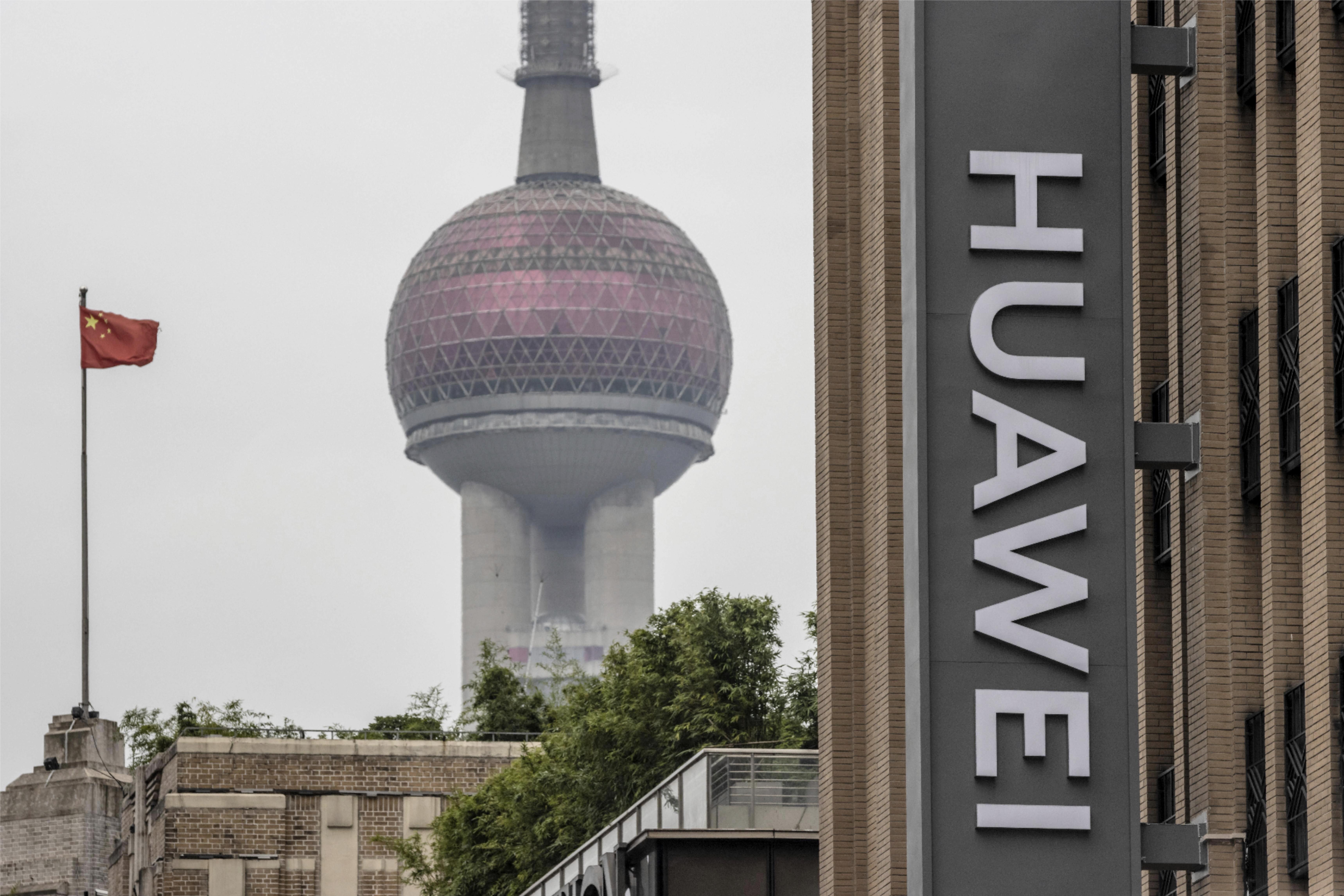
Located in the western Qingpu district of Shanghai, Huawei's new research center encompasses spacious grounds housing the primary chip development center and the new headquarters of HiSilicon, Huawei's semiconductor design division. Once completed, the park is set to accommodate over 35,000 high-tech workers, as per the District People's Government in Shanghai.
To entice talent, Huawei is offering salaries twice that of local chip manufacturers. Industry sources highlighted that Huawei has successfully recruited engineers with experience collaborating with top global semiconductor equipment manufacturers such as Applied Materials, Lam Research, KLA, and ASML. Additionally, engineers with over 15 years of experience at chip manufacturers like TSMC, Intel, and Micron are also among Huawei's potential recruits.
The export control measures enforced by the United States in recent years have made it more challenging for Chinese citizens to work for global chip companies in China, leaving Huawei and other Chinese semiconductor enterprises with a broader pool of top chip talent to choose from.
TrendForce has addressed that the export restrictions on semiconductor equipment by the U.S. and its allies pose significant hurdles for Chinese foundries in obtaining essential tools. In response, the Chinese government, in collaboration with local suppliers, is intensifying R&D efforts to produce domestic semiconductor equipment, particularly for 16/12nm processes and smaller.
This has led to enhanced collaboration between Chinese foundries and local suppliers in both R&D and qualification processes. Despite these efforts, China's progress in lithography tools is currently limited to the 90nm node, which remains a significant obstacle in achieving complete self-sufficiency in semiconductor equipment.
Editor:Lulu
▼▼▼
Micron Expects 4-6% Quarterly DRAM Supply Impact Post Taiwan Earthquake
US blacklists 4 Chinese firms for helping military get AI chips
Meta debuts new generation of AI chip
Google unveils Arm-based data center processor, new AI chip
Western Digital confirms HDD and NAND flash shortages, warns partners of higher pricing
Intel, Dell, and HP face lawsuit in France amid legal battle
+86 191 9627 2716
+86 181 7379 0595
8:30 a.m. to 5:30 p.m., Monday to Friday